
Development of my ZX97 PCB designs
The ZX97 was created by Wilf Rigter from Canada. He designed the source ASCII schematics which I discovered on the internet. On my request he was very kind to design a reduced but functional version of the ZX97, which he named the ZX97 Lite. I asked him for the reduction in order to facilitate my PCB design, after I had designed and built the complete ZX97 on 3 separate boards first. Wilf has also helped me when I was debugging my prototypes. When comparing the ZX97 to the ZX80 with ZX81 conversion, you really can see the excellence of design and timing as done by Wilf. He used no capacitors to adjust timing, but based the timing purely on digital logic, which is a much better and more reliable design.
If you are interested in reading the original ZX97 article by Wilf Rigter, dated dec 1st 1997, please click this link which opens in a new window. If you can’t see the ascii schematic properly in your browser, I suggest to copy it into wordpad and changing the font to courier new or lucida console or a similar font which has equal spacing for all characters if you have a linux or apple computer. When I copied the ascii schematic from the Mozilla Firefox browser, I also needed to remove some spaces between the lines.
My first ZX97 full version prototype is not very suitable for users to build, and thus will not be featured at the moment. The reason is that the original prototype was made up from three PCBs that were connected via two flatcables, one with 40 pins and one with 50 pins. The PCBs are a bit too large and the ICs are not as well distributed as they could be. At the time I was just starting to do this kind of designs, and if I were to design it again today, it certainly would feature a single PCB instead.
The ZX97 Lite prototype was almost without bugs when I finished building the first version PCB. I had a few small bugs related to the memory decoder and extended character set but they were ironed out in the revised designs. (these have not been prototyped because of the nature of the bugs and the fact that I easily could hardwire these small changes on my original ZX97 Lite prototype PCB)
ZX97 Lite
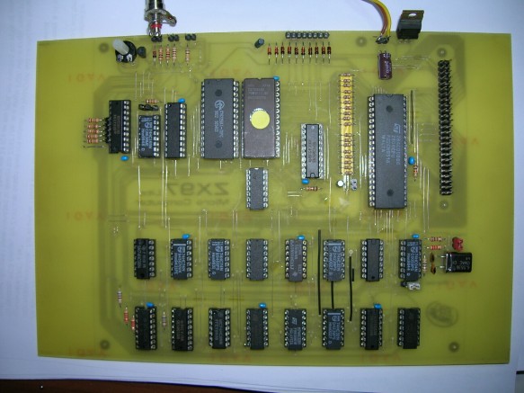
the ZX97 Lite as built by Pasquale from my PCB design
As stated before, the ZX97 Lite is very similar to the ZX81 by Sinclair, of which there is already a lot of information available.
For example, I have even seen a typed text version of the ZX81 manual somewhere.
To facilitate PCB design, the ZX97 Lite design does not include the RAMDISK and parallel port features.
With these changes I have managed to design the ZX97 Lite on a single PCB, with a single sided PCB design.
The PCB measures 15.7x18cm. There are 24 ICs on the PCB, not counting the optional voltage regulator.
Display Type
The ZX97, just like the ZX81, produces a black and white screen on a television set. I have included two jumpers in the design with which it’s possible to select the border and background color. (also see jumper descriptions)
Normally the ZX97 Lite operates in a character mode which means that only characters in the CHR$ set are displayed on the screen, however since the ZX81 has been introduced, several High-res software solutions were invented that allow a high resolution display on the ZX81 of which every pixel is seperately programmable. These high-res methods are also possible on the ZX97 computer.
Tape or no Tape?
In the original ZX97 ASCII schematic the I/O circuits needed for saving programs on a cassette tape were not included, so I used the ZX81 equivalent circuits for tape I/O.
It’s also possible to use the tape input/output signal as a digital serial output, which means that all the tape signal filtering R/C circuits would not be necessary since all signals would be digital TTL level. If you intend to make use of this digital method you could leave out the filtering components C5, R12, (not R11!), R13, C6, R14 and C7. When you look at the ZX97 circuit you will notice that by taking out these parts, you will need to solder in a few wires to connect the circuits to the mic and ear outputs. The component positions that will need a wire soldered in are: C5/R12, C6/R13.
If you do plan to use regular audio devices for saving and loading, you can leave in the parts mentioned and just go with the circuits as in the circuit diagram. I did use a different value in the circuit diagrams for C6/R13 because with the R/C values as in the original Sinclair schematics of my ZX81 kit, I had problems recording programs through the MIC output. After some experimenting I got good results with the values as in the ZX97 circuit diagram.
Also there may be problems with the keyboard being slightly unreliable especially with long keyboard wires (capacitive), and also with loading programs from tape or PC. These problems could be solved by using a 74LS245 for U16, which is the input port for both keyboard and tape input.
Keyboard
For those not familiar with the ZX81 hardware, the keyboard that is used with both the ZX81 and the ZX97 Lite is called a matrix keyboard. This means that all the keys used are mapped in a matrix position. When a ‘row’ line is connected to a ‘column’ line by a keyboard switch, it will be registered by the computer and the action that goes with this keypress will be executed by the computer. The ‘row’ signals are located in J3 and the ‘column’ signals in J2.
The row signals of J3 are then devided in two groups of 4 signals that pair up with the 5 column signals of J2 to make a block of 4×5 keys. Two of these blocks then add up to 40 keys total. The matrix keyboard is more clearly illustrated by the following table:
Block1  J2-1: J2-2: J2-3: J2-4: J2-5: Block2  J2-5: J2-4: J2-3: J2-2: J2-1:
J3-4:     1     2     3     4     5     J3-5:   6     7     8     9     0
J3-3:     Q     W     E     R     T     J3-6:   Y     U     I     O     P
J3-2:     A     S     D     F     G     J3-7:   H     J     K     L   Newline
J3-1:   Shift   Z     X     C     V     J3-8:   B     N     M     .   Space
Please note: most keys have several functions. These functions can be selected by the following methods:
1. Shift + Key
2. Shift + Enter: changes the cursor into a ‘F’ which is the ‘function mode’. In this mode, most keys have extra functions that are accessed by simply pressing the key after you have changed the cursor to ‘F’. After pressing a key, the ‘F’ cursor becomes a ‘K’ or ‘L’ cursor again.
3. Shift + 9: changes the cursor into a ‘G’ which is the ‘Graphics mode’. Keys pressed with a ‘G’ Cursor will result either in inverted text or in combination with shift some of them produce graphic symbols. The ‘G’ cursor will not change back by itself, you will have to press Shift + 9 again in order to change back to normal typing mode.
4. ‘K’ cursor mode. This mode results in a Keyword when certain keys are pressed.
5. ‘L’ cursor mode. This mode results in Letters when you press the letter keys. You can however still use Shift+Key and ‘F’ + Key in this mode which in some cases also produces keywords and functions.
Also note: the ZX97 Lite(as the ZX81 does) handles the ‘K’ – ‘L’ cursor transitions automatically. For example, when you enter a keyword with the ‘K’ cursor, it changes to ‘L’ and you’re able to enter variables, mathematical symbols etc.
Jumpers
J9 selects border color, and J8 selects character color, however note that J8 inverts the setting of J9 if changed.
For example, set both jumpers to 1-2 to make sure you can see the picture on the tv screen because with certain settings can be difficult to see the tv picture.
Make sure you have the memory option jumper J11 closed at power-on because this selects ZX97 ROM in the 0K-8K region.
At power-on, you will need the ROM to be present at 0K-8K because at power-on reset the Z80 starts executing at adress 0000h.
J11 can be used to first load alternative OS software in RAM region 32K-40K (8000h-9FFFh, J11 closed) and switch it to the 0K-8K region(0000h-1FFFh) by opening the jumper. In closed position the ZX97 0K-8K ROM area will be loaded.(which is mostly the same as the ZX81 ROM)
It’s possible to load the OS in RAM region 32K-40K, switch the ZX97 Lite off, change the jumper and switch back on, but this will require the backup battery to be installed on the PCB. (else the RAM contents is lost at shutdown.)
Also have a look at the memory table below.
Jumper J4 selects the TV standard: 50Hz (PAL, for example in Europe) or 60Hz. (NTSC, for example in the US)
Memory decoder
The ZX97 memory decoder operates as follows for the main memory blocks:
Memory-map:
Mem Area: 0000-1FFF 2000-3FFF 4000-5FFF 6000-7FFF 8000-9FFF A000-BFFF C000-DFFF E000-FFFF
Normal:	     ROM	RAM  	 RAM 	   RAM 	     RAM 	ROM 	 ROM 	   ROM
/M1 low:     ROM 	RAM 	 RAM 	   RAM 	     RAM 	ROM 	 RAM* 	   RAM*
J11 Open:    RAM** 	RAM 	 RAM 	   RAM 	     ROM** 	ROM 	 ROM 	   ROM
* during /M1 low, and certain other signal conditions, DFILE is read from RAM, and memory access to the C000h-CFFFh area is redirected by the memory decoder to the 4000h-7FFFh RAM memory area.
** these memory blocks are reversed in relation to the ‘Normal’ situation in he table. (see comments on jumpers)
ZX97 BASIC Keywords
I will search for a scan of the ZX81 keyboard which covers most of the keywords, functions etc. for the ZX97.
There are however several extended ZX97 keywords. They imploy some of the extended functions of the ZX97.
I will add some information here about these functions later.
PCB Layout
If you wish to build this project, feel free to email me. I will then send you the PCB design file. This helps me to know how much interest there is in the project. Additionally, if you have any questions about the project, feel free to ask me.
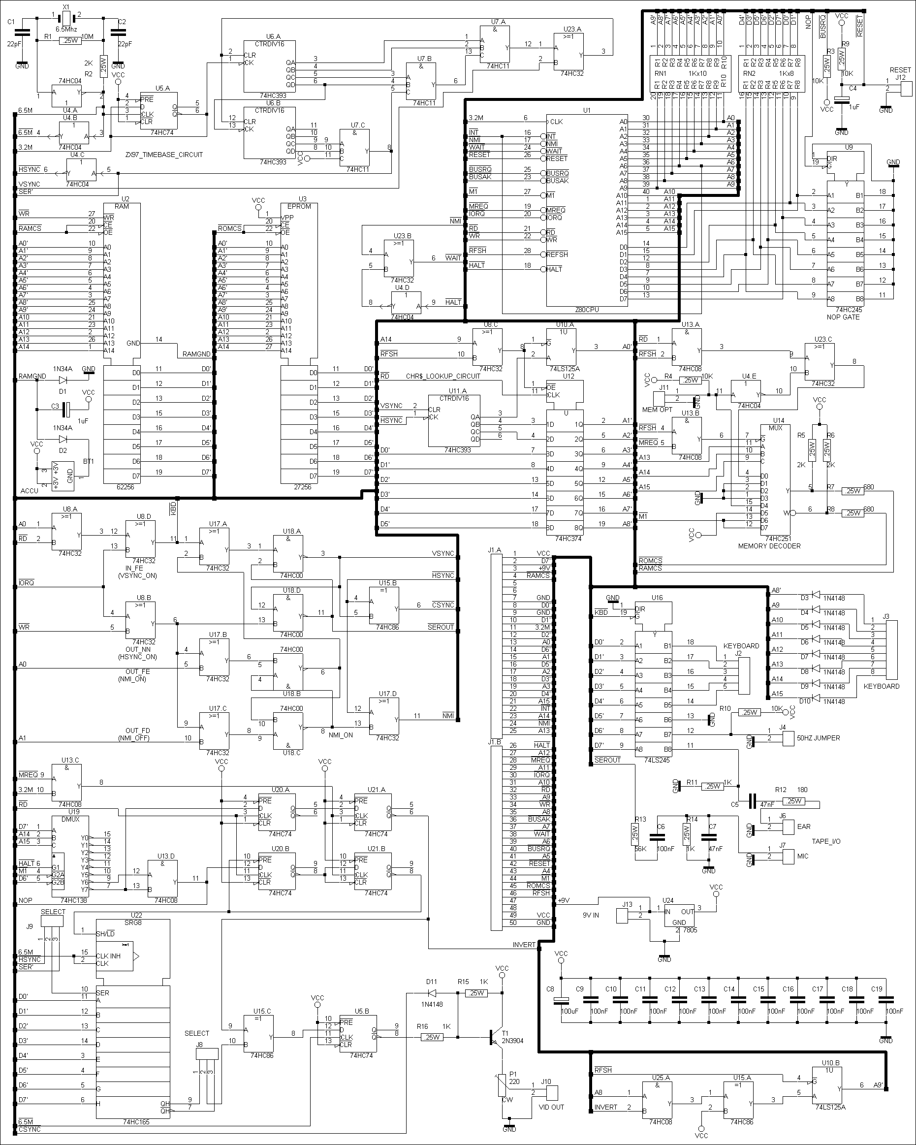
ZX97 Lite Schematic
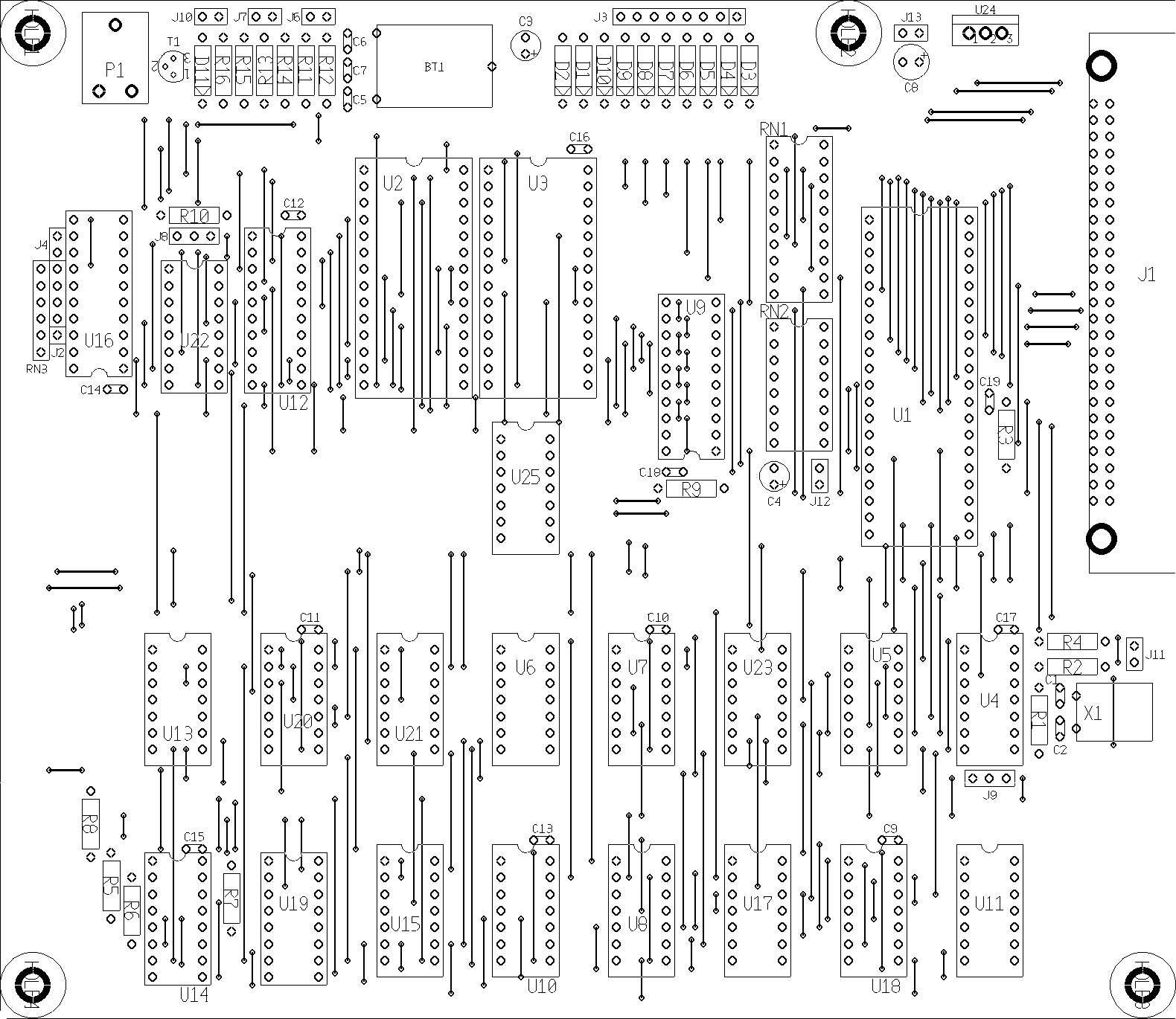
ZX97 Lite Component Placement
The copyrights of Sinclair Technology are the property of international computer manufacturer Amstrad. It is not allowed to use any designs provided in this website and/or any Sinclair Technology found elsewhere on the internet for any commercial use. It is not allowed to sell computers built with or based on plans from this website with the intent to make any commercial profit or gain. The sole purpose of the designs in this website is to use the designs for your hobby or for non-commercial learning purposes.