
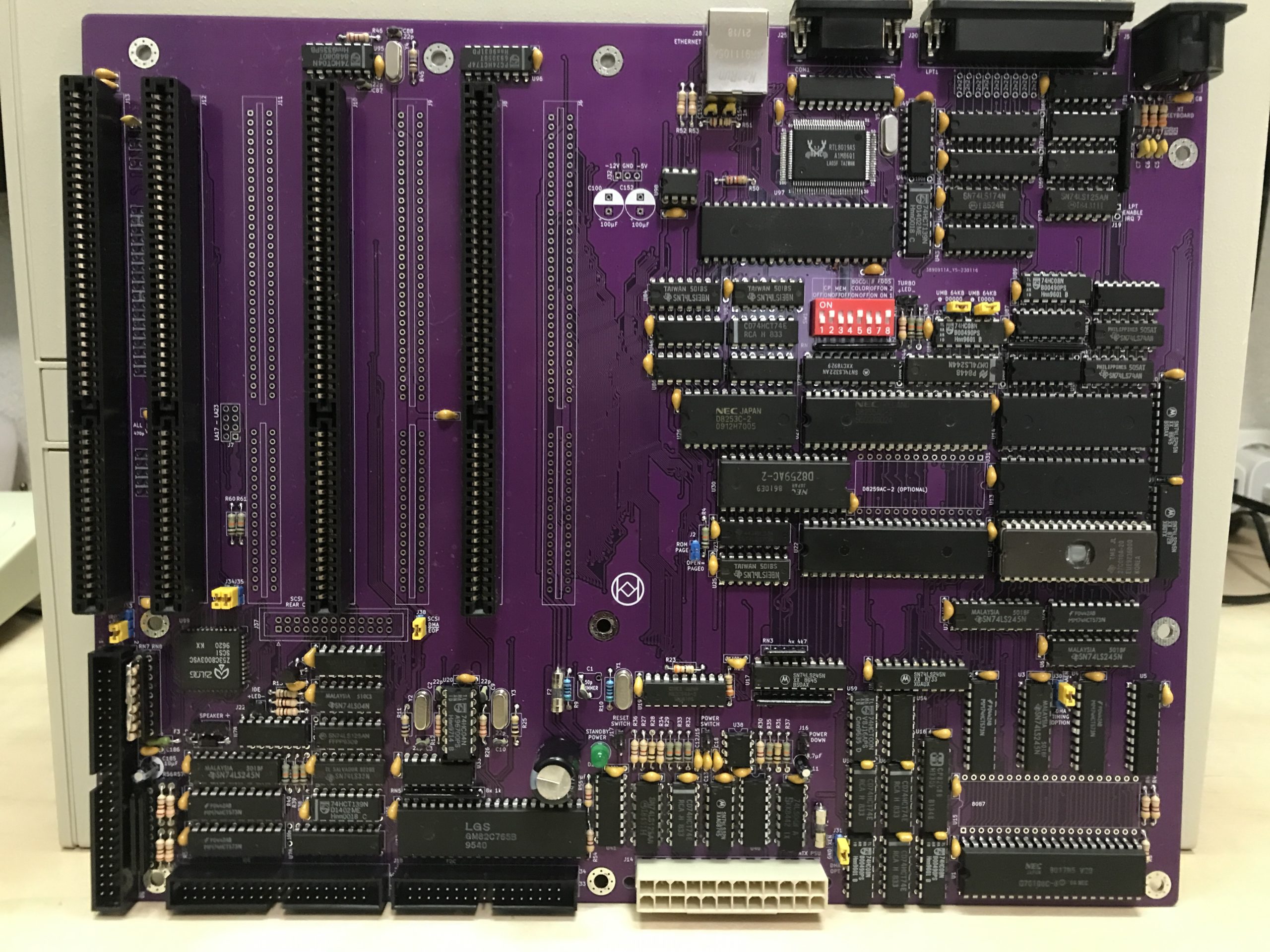
Second Revision XT PC design
As I was testing my first revision XT PC (see the project page of the first project) I have been testing a Future Domain 8-bit SCSI adapter with some CD drives and harddisks. I found these to be still functional and a reliable means for quick bulk file transfers. I could swap a SCSI harddisk with external 25 pin connector between this XT and another PC which contains a SCSI adapter, and this created an external swappable drive for large transfers. The XT doesn't feature USB drives so SCSI is a great alternative for this purpose, I can recommend it. I thought to myself, SCSI is so useful in an XT, it should contain it by default in my designs.
I researched a little about early SCSI development history and found various SCSI controllers which might qualify for a design. The most excellent Future Domain VLSI controller chips are not easy to obtain, so I tried to find an alternative. NCR developed the 53C80 SCSI controller chip, however this chip is also rare to find so far. After a little searching I found a SCSI card on Ebay with a Zilog Z53C8003VSC which is basically a 53C80 compatible chip. This chip is still available for purchase, so I decided to order a few and base my design on this chip. The basic SCSI design is pretty straightforward and after studying the datasheets I have drafted a schematic of a 8 bit SCSI adapter based on this Zilog chip which I believe should be functional. I believe this design might be supported by the "SCSIworks! Version 1.2" MS-DOS software package which I also found on the internet. Of course, I need to confirm this after building and testing the design and will report my findings on this blog page.
The NCR 53C400 in comparison
Since I am doing some research and testing on SCSI implementations for my XT system, I obtained an 8 bit SCSI card based on the NCR 53C400 SCSI chip which only contains an external SCSI connector, no internal one, and doesn't feature a BIOS ROM socket. I have extensively tested this card after receiving it, and studied the excellent datasheet on the chip. It turns out that this 53C400 chip is quite different from what I expected how it operates. Instead of I/O mapped I/O, it uses memory mapped I/O, because NCR attempted to replace the need for DMA transfers by including some small buffering on chip and external SRAM buffering control as an option. Memory mapped I/O means that the chip plugs onto the ISA memory bus and maps itself somewhere in the upper memory area in the C or D segment. Decoding is done on the chip itself, and it even features 3 inputs for selecting the address space. If a BIOS ROM is used on a card with this chip, the BIOS chip will also be mapped in the same region of memory space where the adapter registers reside.
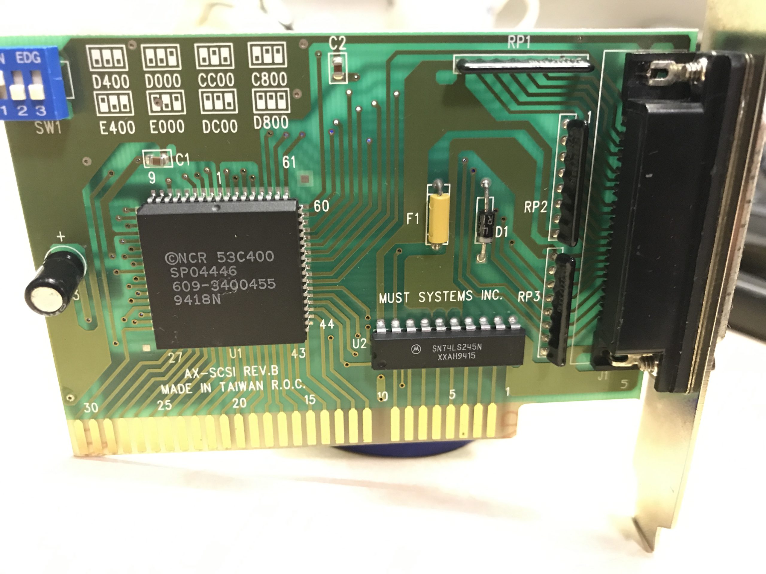
A very simple 53C400 based SCSI card with only an external SCSI bus connector. This solution works really well on an XT PC for backing up and transferring files to an external harddisk.
All circuits in the above adapter are integrated into the 53C400 except the databus transceiver, but control of the transceiver is done by the 53C400 itself.
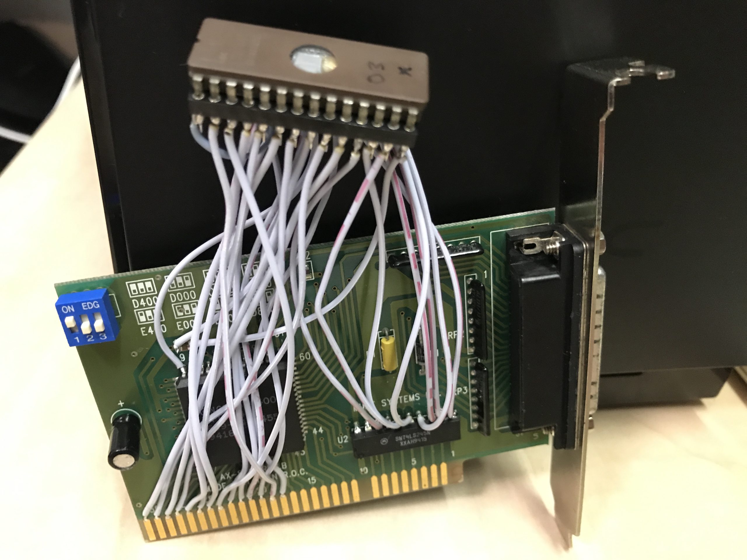
Boot ROM support is always present on the 53C400 so I added a socket to the board for testing various ROM software on my XT and on an AT PC as well.
If anyone has bought a card with this chip and wants to find a driver, you first need to check whether the card has a direct and simple implementation as intended by NCR. If the card in question contains a set of PAL and GAL programmable logic ICs, chances are that the card has changed the function of the SCSI chip to become (partially) I/O mapped I/O, which will need a different driver. Often this will be a branded card so you need to find a different driver.
SCSI support on an XT PC
The issue with supporting any SCSI solution on an XT computer is complicated by the fact that the software needs to be supported by an 8088 CPU, and in my testing experience there are further difficulties with SCSI boot ROMs in that these disrupt the cooperation between the XT PC BIOS, the XT-IDE boot ROM code and Sergey's HD floppy BIOS. In my configuration that I am using I already found that Sergey's HD floppy BIOS is not accessible by F2 key which is normally the case with the ROM software. But this is only a small limitation since the configuration is clearly documented and only needs an alteration of a few bytes in the ROM code. Previously, I have already done such a modification to gain switchable HD and DD 5,25 inch floppy drive support by using two versions of the ROM code.
BIOS issues are always troublesome and depend on how a BIOS works, how compatible it was made for the use case. In case of an XT it's especially difficult because the standard code only supports DD floppy drives and this needs the additional ROM software by Sergey to fix that. So we have the system BIOS, the XT-IDE and the HD-FDD BIOS which have to play nice together, and added is a SCSI BIOS as well. So in my opinion, on an XT, it will be preferable to not be needing any SCSI boot ROM installed. This was already my experience with the Future Domain TMC-950 controller.
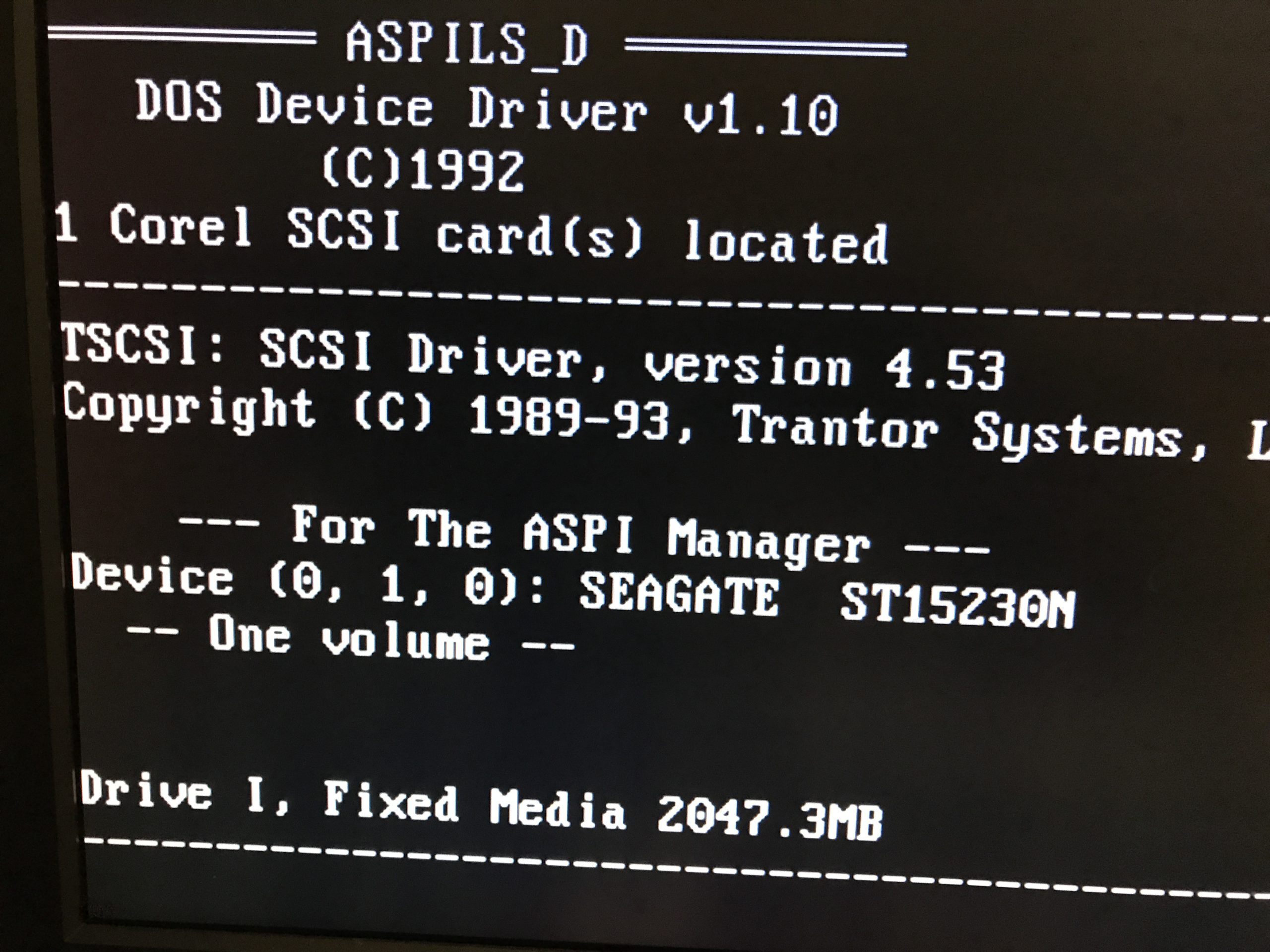
It's by far more useful and flexible if we can simply use a SCSI DOS driver which is loaded from the XT-IDE installed DOS. There still remains the issue of supporting the 8088 CPU and XT system in the drivers of course. Many factors, so it took me quite a few tests and modifcations, I even added a ROM socket to the card with wires for testing different solutions. Indeed, this offered the option to boot from SCSI on an AT PC and adding the SCSI harddisk to the PC INT13 drives without needing to load a driver in software, but on the XT the option ROM froze during loading. The ROM code I found and tested is all somehow not compatible with the 8088 CPU. After further testing however, I found one ASPI driver to load successfully on my XT system without a SCSI ROM, which is the LS2000 ASPI driver, ASPILS_D.SYS. Disk support for accessing SCSI partitions in DOS can be realised by using the older version of TSCSI.SYS, TSCSI.453 (NCR/Trantor SCSI Works 1.2 which works best. It can be found on diskette 1 in the folder OLD. In fact, this solution with these two drivers works so well that it's even 10 times faster to detect and load than the Future Domain ISA card I previously tested. In fact, this code loads fastest of any driver code I have seen on my XT, including CDROM drivers! So I am extremely pleased with this result. You can use TFORMAT.EXE to partition and format a SCSI harddisk, and for example SCSITEST.EXE to scan the XT for any SCSI cards present and supported with a correctly loaded ASPI driver. There is also some tool called SS.EXE which can scan the SCSI bus and show what's connected.
If you have another PC with SCSI, you may try to format the SCSI drive on that PC if it can have more conveniant forms of partitioning and formatting available to create one or more 2GB FAT partitions. I use a Seagate Hawk 4GB SCSI drive which is supported fine in DOS with two 2GB FAT partitions accessible with the above card and mentioned drivers.
Super fast loading of ASPI driver, works perfectly in v1.10 on my XT, now that's really proper programming, whoever did it! Luckily ASPI is a standard which means that the LS2000 ASPI driver can cooperate fine with Trantor/NCR's excellent SCSI disk driver.
Onboard Realtek LAN adapter
After using a Realtek RTL8019AS ISA network adapter on my first revision XT PC, and since I have received some of these Realtek chips from a Chinese seller, I decided to include an onboard Realtek LAN connection on my second revision XT design. I decided to use the 93LC46A serial EEPROM principle for configuration of the Realtek chip. This chip can be programmed in a PC by the Realtek DOS tool RSET8019.EXE, however I was only able to do it on an AT computer so far, for which I can use the existing card to program a serial EEPROM for the Realtek LAN on my mainboard. I will later dump the contents of a few useful EEPROMS for future use. I decided to choose IRQ 3 for the Realtek chip, which also needs to be configured in the EEPROM. I decided against using a boot ROM on this controller chip because I don't like this principle, and I am not sure how reliable of flexible it would be to use this feature for other purposes. If I am going to add an option ROM feature, I feel it's better to directly connect it to the PC bus and use my own decoder for it.
XT IRQ resources are limited, and since I was not using COM2 at all, I decided to remove this port from the second revision design. This freed up IRQ3 for the LAN. I created a jumper to choose between IRQ5 and IRQ7 for the SCSI chip. I found the LPT port to be working fine without using an interrupt. The SCSI chip can use DMA, however I am not entirely sure about what is implemented in the software in order to utilize it. So I made various signals configurable by jumpers, so I can be flexible for testing with SCSI software later. The DMA process in the SCSI controller might also support the /EOP signal from the 8237 DMA controller in the XT PC, so I decided to invert the T/C (transfer complete) signal to add some buffering for safety, instead of directly connecting the 8237 signal. The 8237 is a sensitive chip under certain conditions, sometimes I experienced some crashes when simply touching the plastic top surface of the chip...
Signal integrity on the 8-bit XT expansion slot bus
Initially testing my first revision XT design, I quickly discovered some caveats where it became necessary to apply some additional design care to gain a more stable PC which operates under all conditions. Normally when designing a larger system there first of all needs to be a bus strategy since there will be many chips present on the various signals which will load the bus. For this purpose there is additional buffering present on the mainboard since this is an integrated PC and not a typical "mainboard only" design which needs more adapter cards. Additionally, when designing adapter cards, in my opinion it's good design practice to connect the adapter card to the expansion bus signals preferrably with a load of a single HCT series chip per adapter card. Just to keep on the safe side. More is really not necessary either, and I don't like cutting corners on computer designs, which I believe will quickly develop into trouble which will cost a lot more time and stress to solve after the fact.
I have discovered that indeed the theory of open ended bus lines on a long parallel bus are very prone to reflections and worsening of high frequency noise which appears to spontaniously develop along the open ended bus as it progresses across the PCB. This phenomenon seems to lessen when there are more adapter cards present on the open end of the bus, which places small capacitive loads on the signals which drain off the noise, however the noise on some signals was too large to ignore. I am talking about 900mV of high frequency noise on certain signals, which is simply something I want to prevent, now that I know the level of it. Remember, my PCB is a 2 layer design which by nature has less ground plane and power plane areas than multilayer PCBs. However I still believe a good and solid design is certainly possible in many cases using only 2 layers and some care and awareness. The worst interference was caused and experienced on the RESETDRV line of the ISA bus. Especially UART chips can't tolerate any noise on their reset lines. This intolerance is very subtle which allows for detection of the UART, however when trying to support a serial device on the COM port, things prove to be very buggy and inconsistent. It took me a while too to realise what was going on because at first I suspected an I/O timing problem, which however was proven not to be the case after more extended testing! So I decided to have a detailed signal integrety testing on all of the expansion bus lines. Using some capacitors and a simple but excellently suitable battery powered oscilloscope, I determined a few suitable values for cleaning up the bus signals considerably! This is a subtle process and not to be taken lightly, I decided to use only a capacitor to ground for now, and determined a few suitable values. Already this measure with a suitable capacitor makes a huge difference in what signals look like on a scope. Slow changing lines such as the RESETDRV in my design proved to do well with a 2,2 nF capacitor to ground, while fastest signals such as the CLK signal can only remain reasonably stable using a capacitor of 100pF. Some cases float inbetween these two situations such as IRQ lines, /IOW and /IOR etc which can work well with a 460pF value capacitor to ground on the open end of the expansion bus. Anything larger will make the signal properties change too much which is what we don't want to happen. I am sure that other constructions, such as a capacitor in series with a resistor may produce better results while having less impact on the signal shape, however I also considered the number of parts needed to implement a signal improvement which is reasonable enough. I didn't want to clutter my mainboard layout with loads of components which in my opinion would become overkill measure on an XT computer. So I tried to find the balance between numbers of parts, PCB area and benefit to obtain a cleaner bus. The result is that I added a long row of capacitor footprints on the mainboard next to the outer (left side) expansion bus connector. Probably I will populate all of these. I have not tested this yet, but when assembling the PCB I will attach a scope and retest each capacitor per signal to make sure it will produce an improvement while not interfering with the intended signal shapes and normal operation of the PC. Even though this is a hobby project, one of my goals in my designs is to learn and evolve my design level and instinctive design skill further, so I am finding balance between using more components and their benefits to a more solid design. The more practical experience, the more feeling you can develop for what simply works better. I believe in doing things right, within reason, or else I won't bother to do something at all in the first place. For me there is nothing inbetween, it's just my philosophy in everything.
ATX power supply
Since my last few mainboard designs, I decided to use an ATX power supply to power the computer. After figuring out a basic design which works, I basically copy it onto the next PCB. However, while testing this mainboard I have discovered a complication which arises from having a direct cable connection to another PC with an LPT interlink cable. What happens is that when the other PC is powered up, it features some logic levels on the LPT port. These levels are entering the XT LPT port through the interlink cable. When the XT PC is powered off, it turns out that the 5V power line is slightly raised due to voltages being present on the LPT inputs. The more logic gates are getting this voltage on their inputs, the higher it will raise the power off state voltage on the 5V VCC net on the PCB. Normally this would not pose any actual problem, but here I have an exception. There is a counter chip which I use for my RESET timer. Why use a counter? Well this arose from my earlier tests where I found that relying on a single capacitor charge for timing purposes is extremely basic and troublesome. This was in my case apparent because I was switching off the PC, and then switching it back on before the capacitor was discharged. Adding other components helped a little but was not able to completely eliminate this unreliable aspect in my test circuits. Finally I got fed up with it and decided to use a simple 555 timing clock source and use some counters to create shorter or larger delays, depending on what I wanted. So this counter chip is present in my power on reset circuit. Since on an ATX mainboard we have circuits which work on 5V standby voltage and others which work on VCC, which need to interact with eachother to control the power states of the entire board, and also "power good" monitoring, software power off functions, etc. What happened to cause problems in my case was that this reset timer is powered by VCC, which when connecting the interlnk cable didn't go down sufficiently to reset the counter into its power-off condition, which was however what I need for my ATX circuits to work properly. So after troubleshooting this matter, I decided to lower the counter power supply voltage by 1,4 volts using two diodes in series between the IC VCC line, and using two resistors to ground on each stage proved to decrease the voltage to 0V completely. At first I was led to assume that this was an annoying feature of 4000 series CMOS logic, however after deciding to test using a different counter in LS logic, I found this counter to demonstrate the same problems as the CMOS one. So this is not a "sensitive" CMOS logic problem, but simply a generic design complication which affects various ICs. Perhaps my solution is rather "unorthodox", however I have found my ATX power and reset solution to work really great, so I don't want to switch to an entirely different design at all, not to mention all the hours of testing and debugging which would be involved. I have a solution so I feel it's better to improve the solution than to throw it away. It may seem a little strange to be using several TTL ICs for the power on and reset function, but remember, I am using off the shelf logic to perform this function, and not relying on any programmable controller or custom logic. Thus, my principle is future proof and reproducable in various new forms as well.
BIOS ROM implementation
On this design I have provided the entire XT BIOS address space F0000-FFFFF on a single ROM socket. The socket is designed for using a 128KB ROM to provide more flexibility for future use. The ROM can contain 2 different copies of a system BIOS, selectable by a jumper or external toggle switch. The socket provides for an EEPROM such as the SST39SF010, however I have found during my tests that under certain conditions, for example testing with UMB RAM drivers, the EEPROM may get corrupted which is rather annoying when it happens during testing work. After these problems I decided to use an AM27C010 EPROM instead, and used this without further problems. I can use UV eraser so it's no problem to erase an EPROM if needed. An EPROM is recommended!
The BIOS memory space of an XT is devided into 8kb segments, the upper most segment at the top of the 1MB memory space must contain the Turbo XT bios. Next come the XT-IDE (8k) and Sergey's HD Floppy boot BIOS (8k). Below that I am using 5 blank 8kb segments. I changed a few bits on Sergey's HD Floppy BIOS to create two versions, one version with a HD 5,25 inch floppy drive and one with a DD 5,25 inch floppy drive as drive B. The BIOS can be switched with a toggle switch, and I made a second toggle switch which enables the floppy bus drive select on my DD 5,25 drive or my HD 5,25 drive. Both remain connected but at the moment only one is active at a time. The problem is, a HD 5,25 drive is not suitable nor reliable for using DD floppy disks. There are various complications such as recorded track width which is thinner on a HD floppy which leaves conflicting magnetic information on the sides of the tracks which is picked up by a DD floppy drive. In short, it's not a good idea to read or write DD floppies in a HD 5,25 drive, so in order to read all types of floppy disks, we need both drives. At the moment I have implemented a 2 drive floppy controller on the mainboard. I could create a different drive controller for example like I have seen with two flatcables, or revert to some original scheme of floppy controller, but I prefer to use this method instead, simply turning on or off the drive select on the drive itself. This is a great, simple and flexible way to do it. I just flip two switches and reboot the PC if needed, and I can use both of the 5,25 inch drives transparently and easily from DOS. If I find an elegant way to implement 4 drives on a single floppy flatcable easily, I may still do that in the future. I think the biggest hurdle is not to wire up this solution in a workable way, but to find a compatible BIOS which can configure things in a way which is compatible with the 4 drive straight connection method and supports 4 drives on the floppy bus.
Implemented features on this mainboard
To know what this mainboard contains, here is a list of the components present in this revision:
- 8088 or V20 CPU
- 8087 coprocessor socket is present
- keyboard controller principle is functionally the same as the original XT PC
- COM1 single serial port with GM16C550 and SN75185N RS232 line driver, for example for a mouse
- IBM compatible (PS/2 type) discrete bidirectional LPT port
- XT-IDE compatible IDE port using the double byte "fast" access by putting the two bytes next to eachother in the I/O space
- standard HD floppy controller using a 82C765B by LG Semiconductor, or compatbles such as the WDC one.
- Zilog Z53C80 compatible 50pin 8-bit SCSI bus onboard, featuring a second header for creating a typical 25 pin rear SCSI port using a DB25 female connector on a flatcable.
- Realtek RTL8019AS using serial EEPROM for jumperless configuration, no boot ROM used on the controller
- Discrete ATX power supply and reset timing control including power good monitoring and shutdown, software power down input header is available for designs which want to use some form of software controlled power off function.
- 7 expansion slots (8 bits bus with partial 16-bit interconnections between the slots)
- 1MB SRAM memory. (XT refresh and parity logic removed, however /DACK0 pulse is present and working on the expansion bus for cards which use it such as Trident VGA)
- 2x 64kb UMB blocks D0000 and E0000 available, selectable by jumpers for example in case an EMS paged memory PCB is to be used
- 128kb EPROM or EEPROM socket for XT BIOS at F0000, jumper selectable between 2 pages of 64k in the ROM. For example for alternate BIOS switching. Recommended to use EPROM.
- onboard integrated I/O devices are in most cases separately buffered wherever possible to keep enough load capacity available for driving the expansion bus
- CPU operates in turbo mode (8Mhz) by default while DMA controller, keyboard and system timer circuits operate on their proper independant fixed clock frequencies. CPU can be switched down to normal mode (4,77Mhz) by key combination. DMA clock signal is a fixed 50% duty cycle clock of 4,773 Mhz, independant of the selected CPU speed. This is in my opinion the best way to implement the "turbo" principle on an XT. For example, this design never crashed my PC when switching between normal and turbo modes while it was running, including when any software was running at that time.
- Cascaded 8259 interrupt controllers, currently unsupported in BIOS so one socket is unpopulated for now to prevent locking up the computer at boot. IRQ2 can be easily jumpered on the second socket in case it could be used by some expansion device on a card under certain conditions.
- capacitive signal filtering implemented on expansion lines to clean up signal (reflection) noise
- Standard full size ATX mounting holes and expansion slot locations
Testing and debugging the prototype PCB
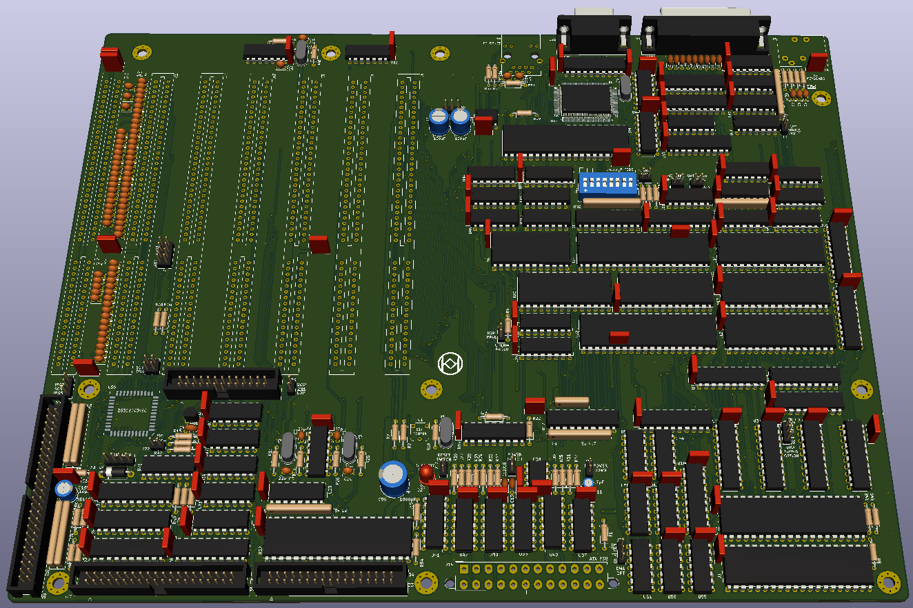
A photo of the assembled mainboard PCB. Most components are directly soldered onto the board. Most of the ICs are recycled old parts from other (useless) old PCBs and first tested in another system before soldering them onto this PCB.
I have received the Revision 2 XT mainboard PCBs and built one up. It powered up and booted immediately without issues. I then painfully discovered how bad some of the Chinese precision type IC sockets sometimes can be when I found some keys not responsing on the XT keyboard. While I was probing the 8255 inputs with a scope, I discovered that the 8255 was so loose in it's socket that I could even move it slightly by hand. When I pressed it tightly in the socket, suddenly all keys worked properly. So after replacing a few sockets things started to work better. However I found some stability problems and the floppy drive access not working. After removing the floppy controller chip and decoder from the mainboard and plugging a few different 8 bit floppy controllers, I also found those not to work. So the problem was more in the system and affected I/O timing in general. After more testing I decided to take an estimated chance. What I did was I decided to build up another PCB, but this time directly soldering almost all ICs into the PCB. I did this because I found some unknown problems and I wanted to eliminate any possible causes so I could focus on real issue. So, I tested every IC of the Rev 2 design in its original location on the Rev 1 mainboard. I then proceeded to solder everything into a new PCB in their respective locations. After completing the directly soldered PCB, I did find the floppy drive function was restored to normal operation. However, there were other stability issues which I found by testing the system in Windows 3.0. I played the game Patience for a few minutes and got some weird crashes and freezes, and even a devide by zero error. So somehow even memory access was impacted by the problem in the system.
Long story short, what turned out to be the problem? The clock pulse line of 24Mhz was apparently experiencing some different impedance from the PCB, which skewed the clock to a slightly lower frequency, which was not a big problem persé I believe, however it also showed some dynamic skewing of the frequency. Of course, if you operate the address lines and request to receive some I/O from a chip of RAM location, if at that very moment the clock pulse slows down or speeds up, you will miss the window of availability of the I/O byte or memory byte on the databus. So that was what was happening to me. I became aware of it when I noticed the frequency of the 24 Mhz and derived 8Mhz CPU clock were slightly off. I experimented on the oscillator circuit with some different load capacitors on the crystal, and found that it needed slightly lower load capacitors to achieve it's resonant frequency oscillation. It turned out that 12pF worked well in this case. I never had this problem before on any computer PCB I have build, and I have built many! Usually I just throw in 22pF capacitors and things always worked with HC or HCT type inverters. Additionally it may be beneficial to use HC04 type inverters instead of HCT04 types, results may vary and can be verified with a scope. Though it was frustrating at first, and came as a surprise since this is already the second revision mainboard, in hindsight I am very happy to have experienced these problems anyway because it also provided some valuable hands-on experience in system design and troubleshooting. Another thing to look at while designing or testing a system. The more problems you experienced, the more you will have learned about how these systems function and which issues require additional attention. I read several application notes and PDF documents about oscillator circuits, quite interesting. I plan to do some experimentation in the future, because I saw that the waveforms on the base 24Mhz oscillator were not shaped like a block waveform at all, but showed something between a sinus and block wave, and the lower frequency derived clock pulses showed clock pulses that look a lot better. So in conclusion the clock pulses in the system are now again 100% stable as I am used to observing in my revision 1 PCB. I added more GND shielding around the clock pulse lines so I am sure this is the cause of creating a higher impedance on the clock line traces, which required me to need to lower the load capacitors. The purpose of load capacitors is to ensure oscillation starts up properly and remains stable for the oscillator. My advice is, just check the clock pulse with a scope, and try out some different values of load capacitors if the clock pulse is not stable or correct. If the oscillation frequency is too low, you can experiment a little, for example lower the load capacitors, if the oscillation doesn't start, increasing them slightly may help as well. That's my experience. With a 24Mhz clock crystal on a 74HC04, I found 12pF to work well enough.
So I proceeded to test the "soldered directly" mainboard, and was surprised how stable it suddenly became after fixing the clock. It's rock solid and I even successfully tested a Trident, Headland and even a cheap Realtek VGA card. All worked fine, though my Headland card is showing some signs of a bad RAM which flutters a few pixels. I will fix this later, I don't mind it that much. The Headland VGA card seems to work best so far, though the Trident card is also nice and well integrated in comparison.
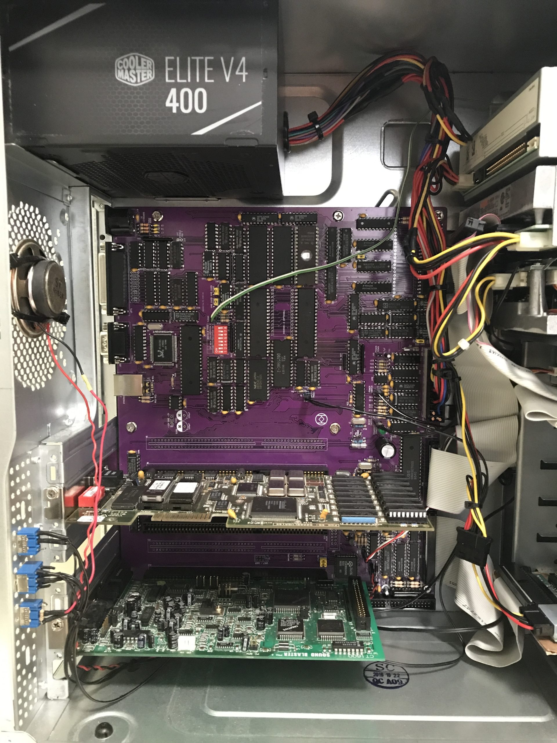
The mainboard assembled into an ATX PC case. This integrated design only needs a video card and soundcard of choice to create a complete XT PC.
I experienced problems again with the UART chip for the COM port just like on the Rev 1 mainboard. It may be the case that the UART chips I am using are too sensitive on their RESET inputs, which is another example to demonstrate that a negative logic /RESET input is more sound design than a positive logic one. The negative signal needs to travel much further down to signal a correct logic level change on the input, which is more safe to protect against slight signal noise on the trace for example through crosstalk between traces or power supply ripples. Anyway, this UART chip is so extremely sensitive that I had enough of it and decided to connect the RESET input directly to a ground plane on the PCB from now on. This chip is really much too sensitive on its RESET input.
The integrated Realtek LAN works really well, no problems at all. I tested it with a Chinese shielded RJ45 socket with integrated magnetics, this RTL8019AS LAN chip really provides a nicely integrated solution on the mainboard, requiring very little space when you look at it on the PCB. Much better than a separate card with lots of unused additions. Using a serial EEPROM to configure the RTL8019AS is something I can recommend. It would be handy to have a Realtek ISA card available with a 8-pin socket for the EEPROM so you can use a 286 PC to program the configuration into the EEPROM, then transfer the EEPROM to the integrated mainboard and you're done. I will dump some example code from the chip after I have experimented with a few different settings to save each version. The physical LAN MAC address is also set in the EEPROM.
I am still waiting for the separate PCB which contains the LAN, COM1, boot ROM socket and SCSI controller design, which is still in transit by DHL. So I will first do the testing of these designs on my mainboard for now until I receive the PCBs.
Moving on to the SCSI controller. I have done some initial testing and have not found a working old driver for the Zilog 53C80 clone chip yet. I came close once with a SCSI driver made for the Mediavision PAS16 sound card which contains the same Zilog chip, I imagine for supporting a SCSI CDROM to provide a multimedia solution with that card. The driver I found to at least detect the Zilog chip on my mainboard is "ASPIMED.SYS" in the SCSI! driver collection package, using the CONFIG.SYS line: DEVICE=C:\TSCSI\ASPIMED.SYS /P0320,05 /RW which selects I/O port 320, IRQ 5 and resets the SCSI chip and waits a few seconds before proceeding to load the driver into memory. If I don't connect any drive to the SCSI bus, the driver seems to work normally because it then only looks at the SCSI chip itself. However when I try to poll a SCSI device on the SCSI bus in DOS after loading the ASPI driver, I am getting timeouts. Possibly, the configuration of the Mediavision card is using some additional logic somewhere on the sound card which is not present in my design. I have seen SCSI adapters which use a transceiver chip on the SCSI bus data lines for example, which I solved at one time before by removing the transceiver and putting in some bridges to the data lines. According to the datasheet, the SCSI chip is more than adequate by itself to drive the current for the SCSI data lines on the bus. After removing the transceiver, the card worked fine with the driver I was able to find. Now my situation may be the reverse, I am not sure yet, so I am searching for some other old ASPI DOS driver which hopefully can work with my SCSI designs. I need to do more searching and research on this. I know there is one 8 bit card based on the Zilog SCSI chip made by Nolan Computer Systems, the NCS-250-SC. However so far, I only found a driver for windows 95 for this card, not for DOS mode operation. If anyone knows a driver which may work in my case, feel free to send me an email. If I can't find any functional driver, I may abandon this chip and move to a different SCSI chip for my designs, but I will make sure to own an existing card with that same SCSI chip for testing to make sure I have a working driver. Finding a driver for a 53C80 is not that difficult, however when looking in more depth at different cards, there are many circuit variations made using this chip on various SCSI adapters which depend on other logic and ICs. This eliminates those drivers to be suitable for my designs. I think the Nolan Computer Systems card is the most comperable with my design, it also seems to use the datasheet as a design basis when I look at the components used on the card.
Another design I have made is an EMS RAM expansion using 4MB of SRAM chips to expand an XT's memory with 4MB, to be paged into a 64k page on a selectable frame window. The EMS adapter is similar to certain Z80 8-bit CP/M systems with larger paged memory space(similar to for example the ROMWBW principle). So I chose to use the 74LS670 paging register chips for my version of this card as well. The EMS adapter PCBs have been delivered, I will finish building and testing one soon.
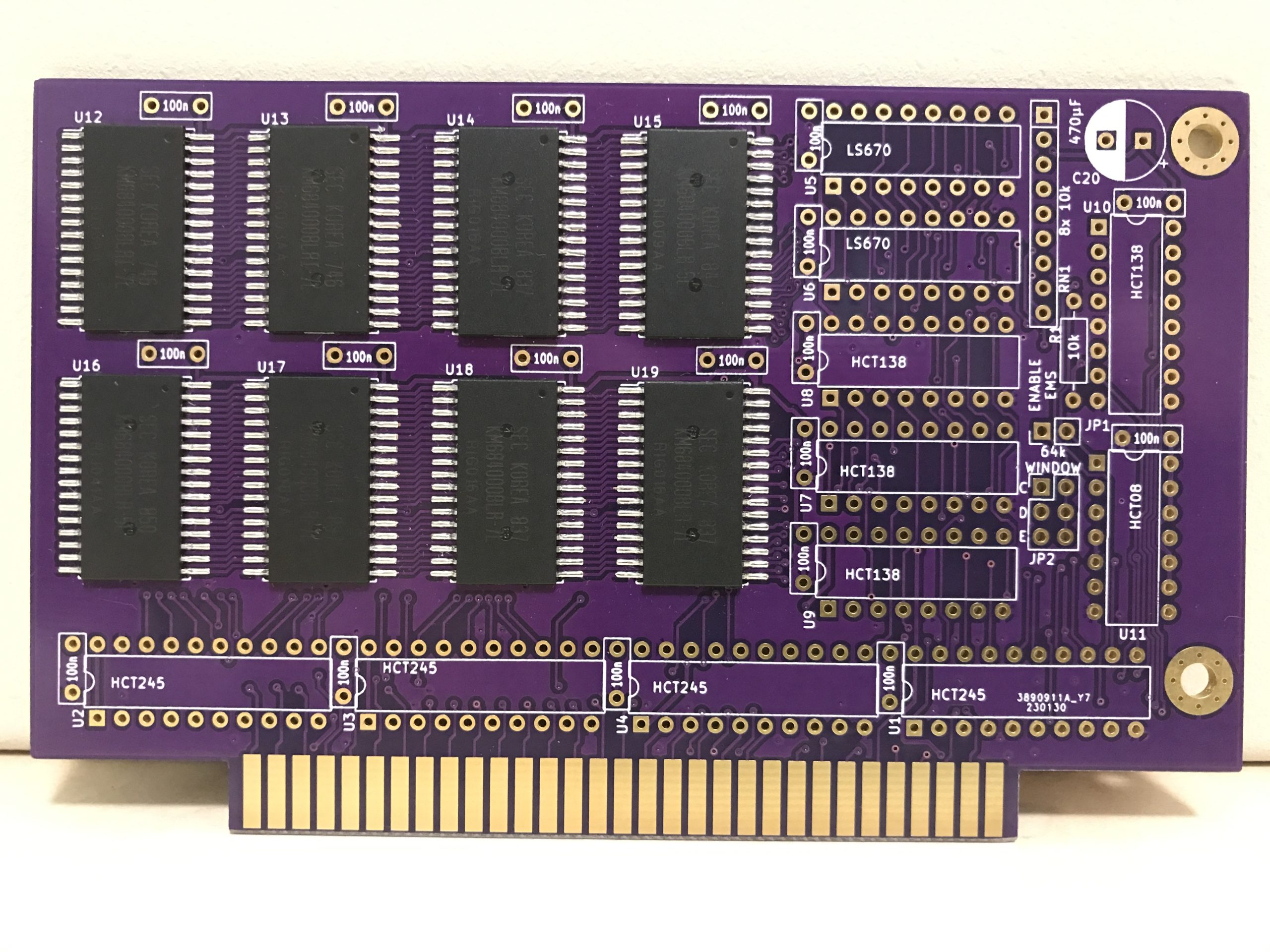
A photo of the EMS memory PCB with 4MB of SMD SRAM chips soldered. I enlarged the SMD pads to accommodate most of the 4Mbit SMD SRAM IC packages available with this pin spacing.