For a long time I have been studying schematics and documentations of the original IBM 5160 XT PC and generic XT PC clones from Taiwanese manufacturers. The more I studied these schematics and compared between IBM designs and clone manufacturer designs, I gradually formed a plan to build my own recreation of an IBM compatible XT mainboard. My motivations are especially from a historical viewpoint, and to gain an experience and insight into how IBM created the worldwide industry standard for PCs, the choices they made, and how and why this standard became so popular. In recreating this design and using the resulting PC, this can give an interesting perspective and insight into computing history and the success of the IBM compatible PC. Various parts of the original IBM design are still present today in even the most modern PCs. For example check your system clock IO address in Windows 10, it’s still the same!
The creation of my own schematics in KiCad has been a process that lasted a few months in my spare time. To me, doing this kind of design and working out these plans is a form of relaxation, which I much prefer to other alternatives since this activity also can result in an actual concrete design which has proven to be informative, educational and insightful.
I gradually assembled my own schematics of an IBM compatible PC, where I attempted to combine the benefits of the IBM industry standard, and to find a combination of the most useful circuits and features. While making the design it was obvious that the IBM compatible PC is a complicated computer, when compared to other systems of the time, though arguably not the most complicated system imaginable either. It’s interesting now to study the background of IBM’s process, which I will research more on after my newfound experience in realising this design. This design is purely educational and it is expressly not permitted to form any commercial product on these designs. It’s not to be deemed to be fit for any purpose or function and purely to be seen as an historical experiment. Building such a computer can only be done with expert knowledge and experience. If you even remotely doubt your experience, you should not attempt to build this PC without professional supervision! Anyone building this project, agrees to do so at their own risk and responsibility!
Design features
Basic features of my design which are worth mentioning are:
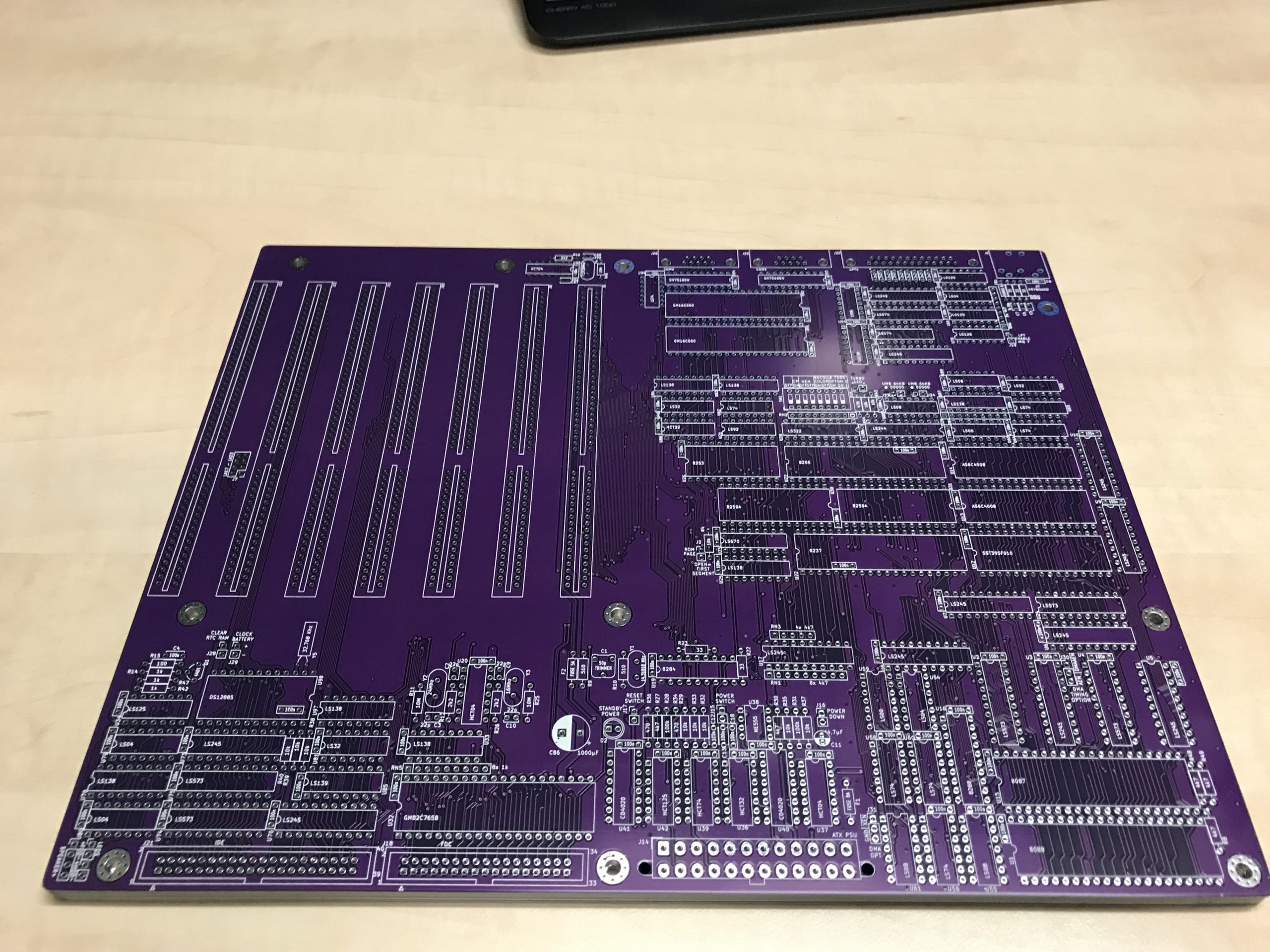
- ATX form factor PCB
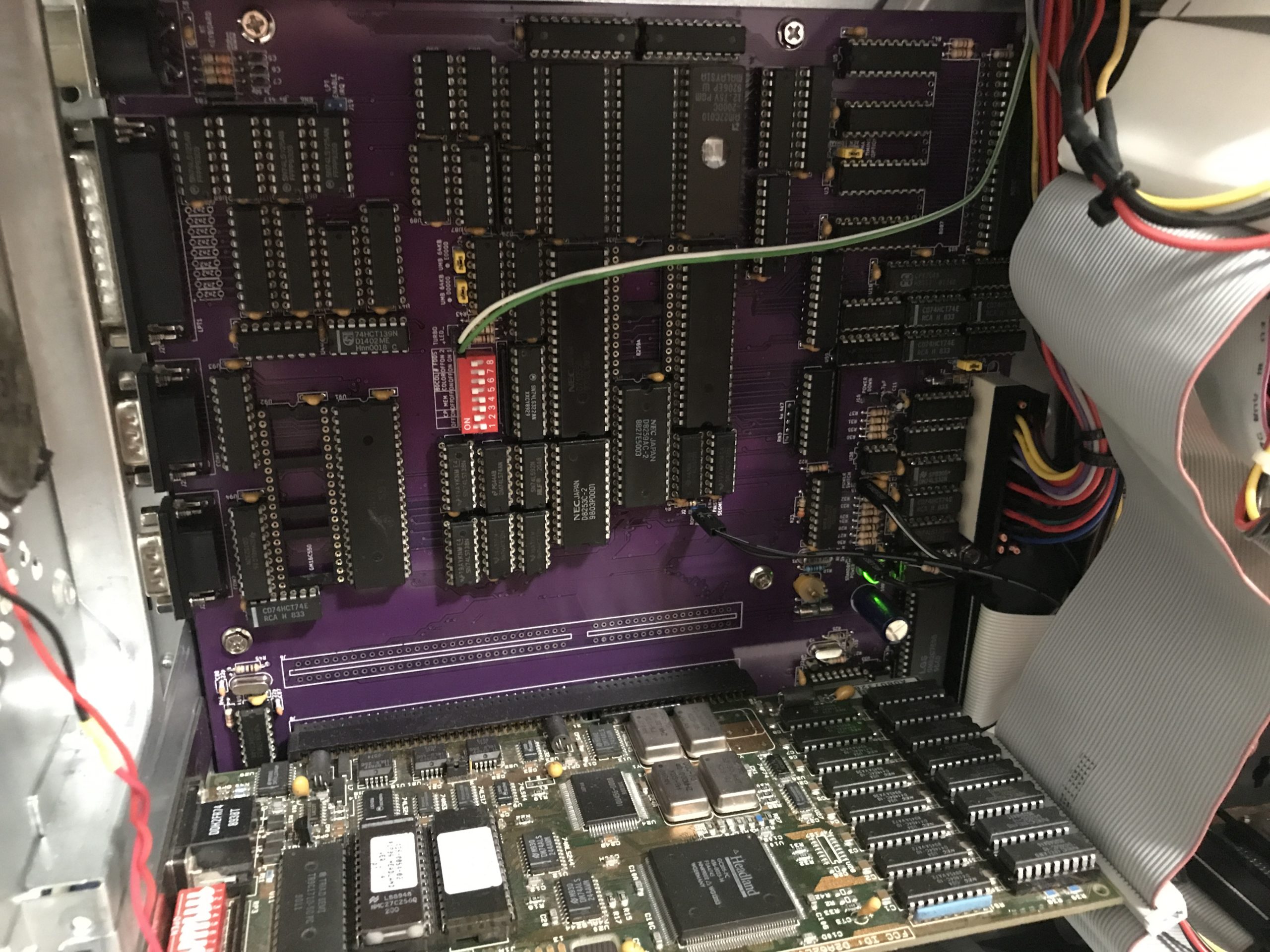
- 7 expansion slots, 8-bit XT system control using 16 bit physical ISA slots
- ATX power supply control (my own circuits)
- power on reset timer (discrete circuits of my own)
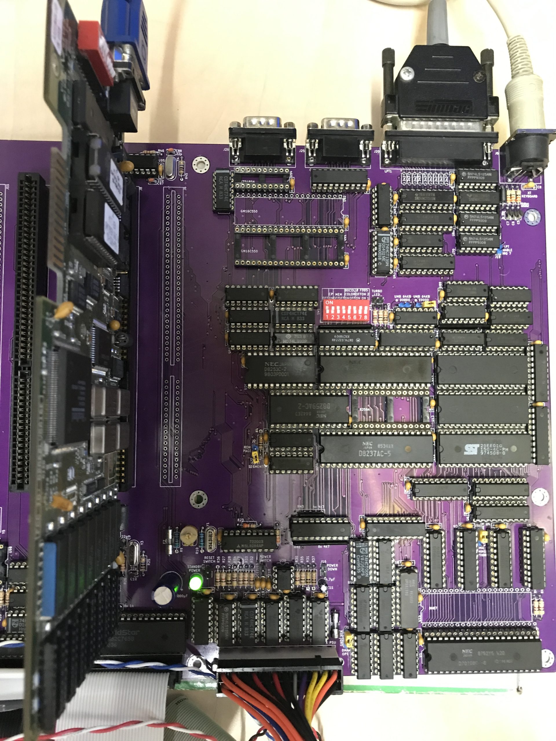
- IBM PS/2 style discrete bidirectional parallel printer port recreation (LPT1)
- dual 16C550 serial communications ports (COM1, COM2)
- original XT style keyboard control using 8255 PPI for originality, slightly modified circuits
- original XT dipswitch for settings using the 8255 PPI
- XT-IDE compatible IDE interface (my own variant of the XT-IDE circuits)
- standard HD floppy controller
- dual Intel 8259 interrupt controllers, however not yet implemented in BIOS so I didn’t populate the second cascaded controller yet, the circuits are prepared for future implementation, needs ROM modification
- Intel 8237 DMA controller and supporting logic implemented
- 8 bit PC IO Channel bus arbitration logic, adapted and updated version using common logic chips
- full X-bus implementation in similar functionality as invented by IBM. Circuits redone in my own logic in certain areas.
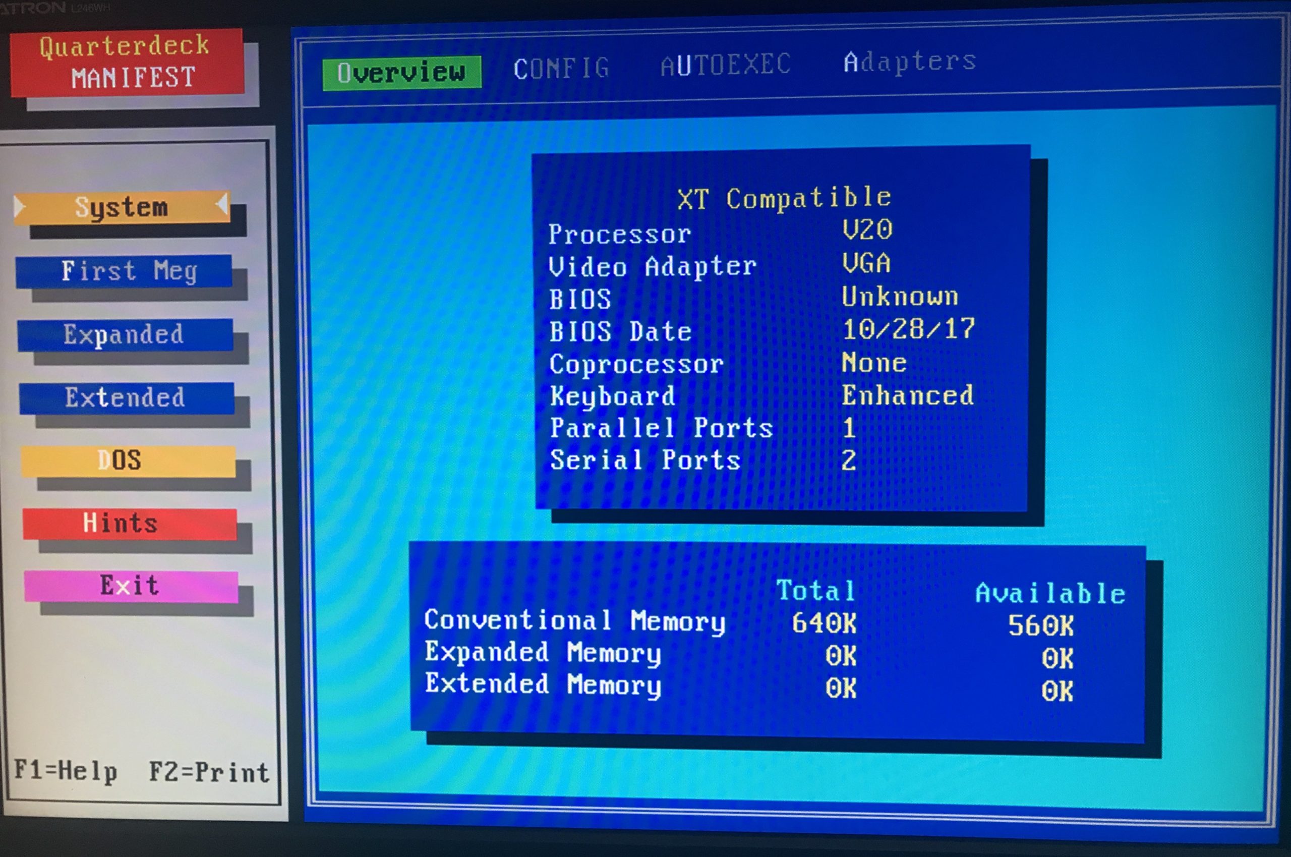
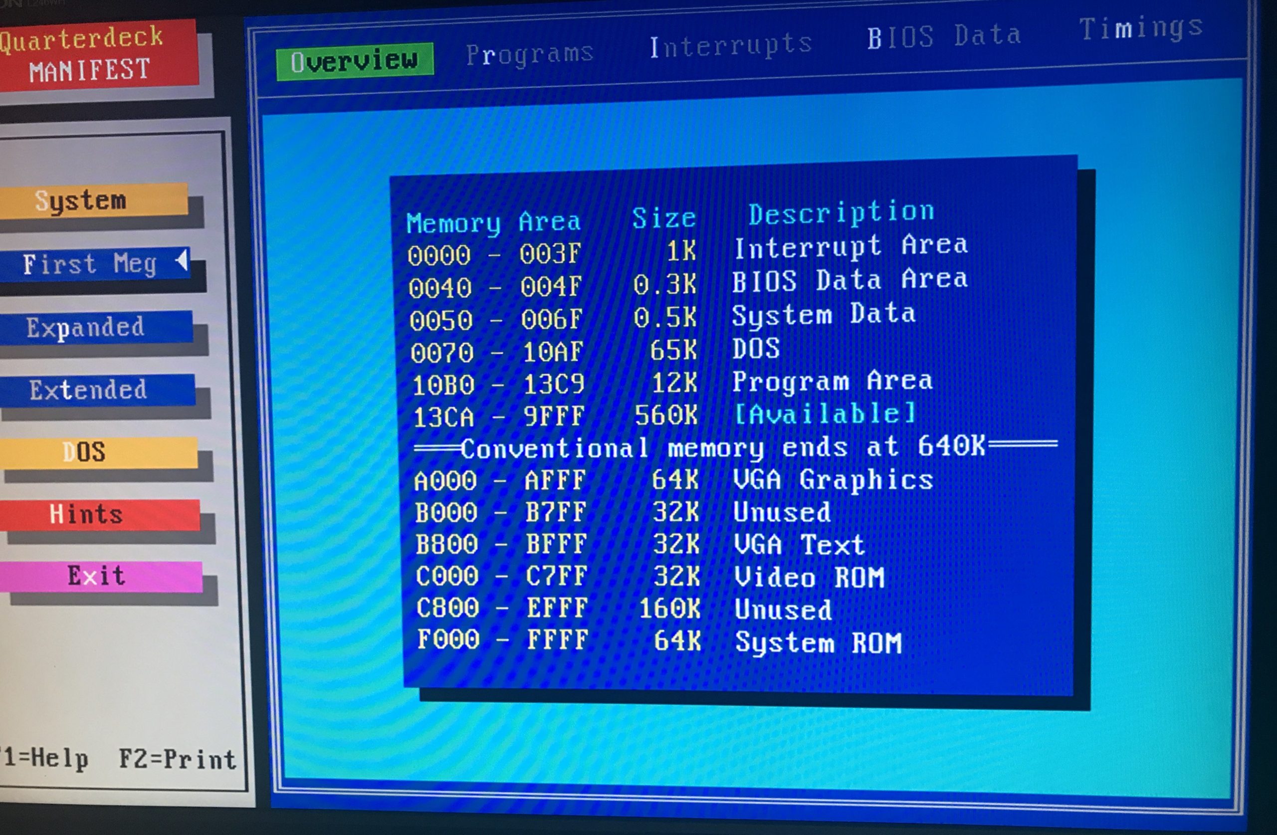
- 640kb SRAM memory, eliminating the need for a lot of the elaborate DRAM demultiplexing and timing/refresh control logic originally used in the IBM XT PC.
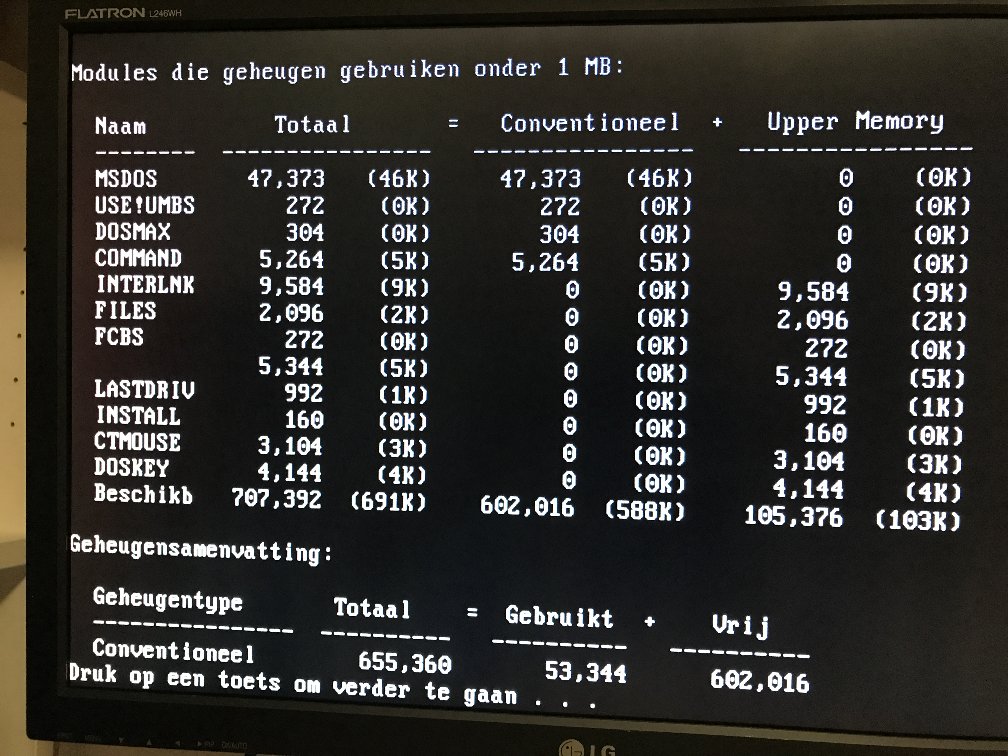
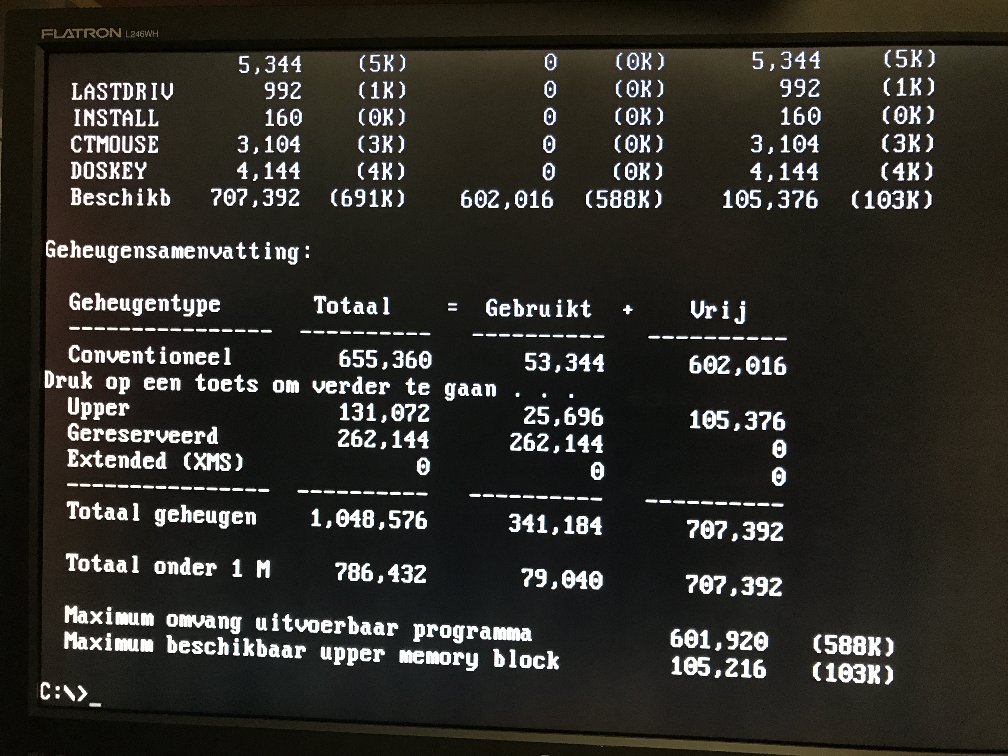
- UMB RAM blocks available at D0000 and E0000 segment locations, total of 128kb UMB RAM memory, fully available for loading drivers and TSRs in UMB area.
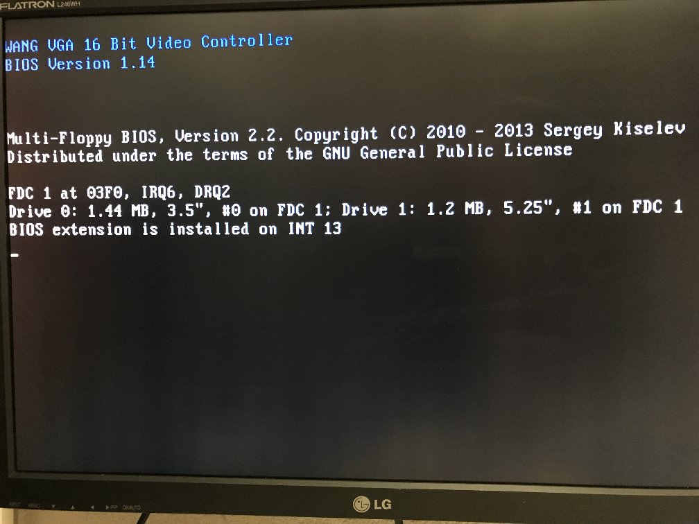
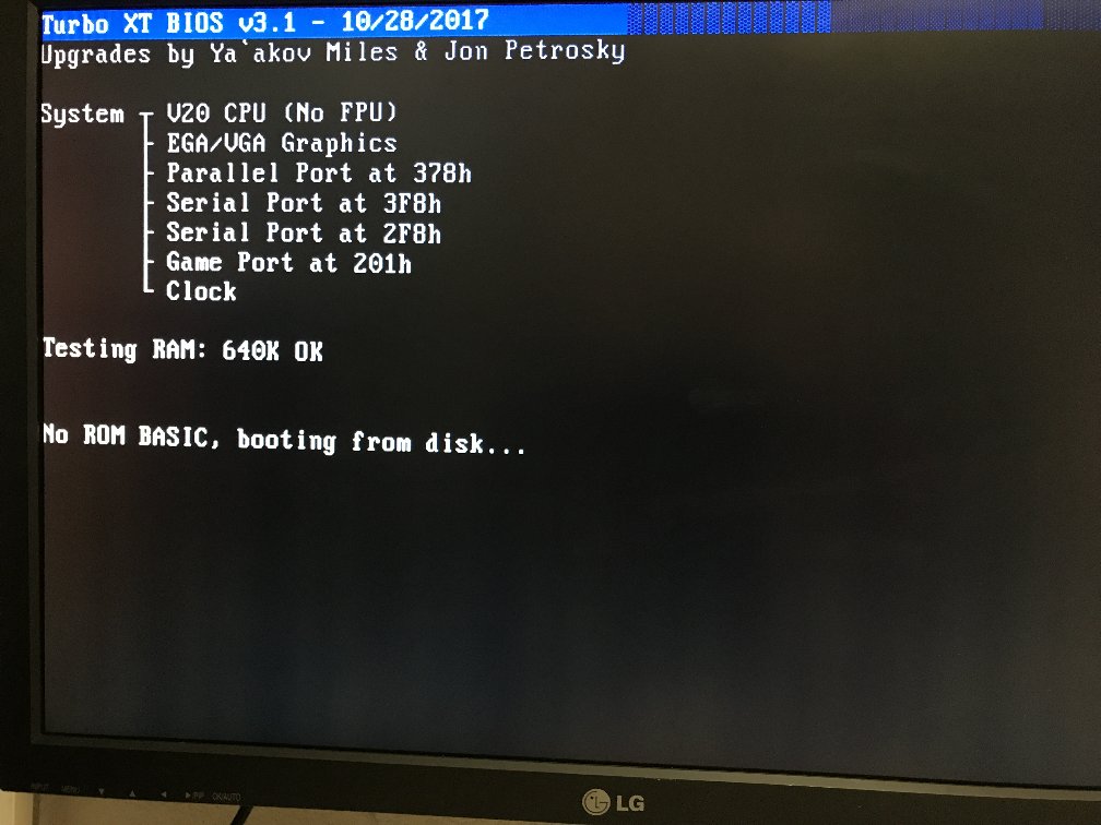
- fully compatible with: Super PC universal XT Bios by Ya`akov Miles (1987) and Jon Petrosky (2008-2017) brilliantly fixing even original 80s manufacturer’s bugs, imperfections and errors in modifying IBM bios code, XT-IDE BIOS by by Tomi Tilli and XTIDE Universal BIOS team, enabling the usage of large capacity IDE drives and formatting up to 8GB storage, and HD FDD BIOS code by Sergey Kiselev, enabling the use of 1.44MB HD floppy drives. Their work is extremely valuable and has elevated the usefulness of the XT clone design to a very high level of user friendly functionality! When powering up an original BIOS of an XT clone mainboard, the boot options are extremely limited without these bios upgrades! Thanks to the hard work done to create modern well developed ROM software, we now have these much better options! All PC BIOS software is in F0000-FFFFF memory location, occupied by a single ROM chip which can be programmed with the joined BIOS code. If the user wants to add more option ROM software, it can possibly be added into this ROM since the 64 kb is not fully in use yet.
- ROM chip is writable, but has occasionally been corrupted by certain exceptional situations in testing conditions, requiring reflashing of the ROM chip. If this happens too often, an EPROM is recommended and can be placed in the ROM socket instead. When using UMB blocks, it’s highly recommended to use an EPROM to avoid corruption of ROM areas.
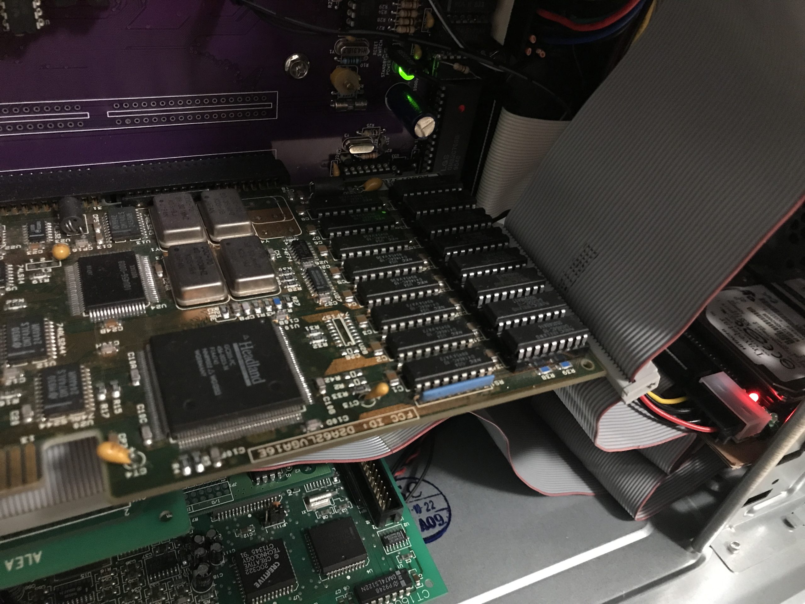
- compatible (so far due to not having many cards for testing) with Trident TVGA9000x cards jumpered in 8 bit mode and Video7 Headland chipset ISA VGA cards. I have also successfully tested a CGA card, which I verified to give a picture on the composite output using the right dipswitch settings on the card
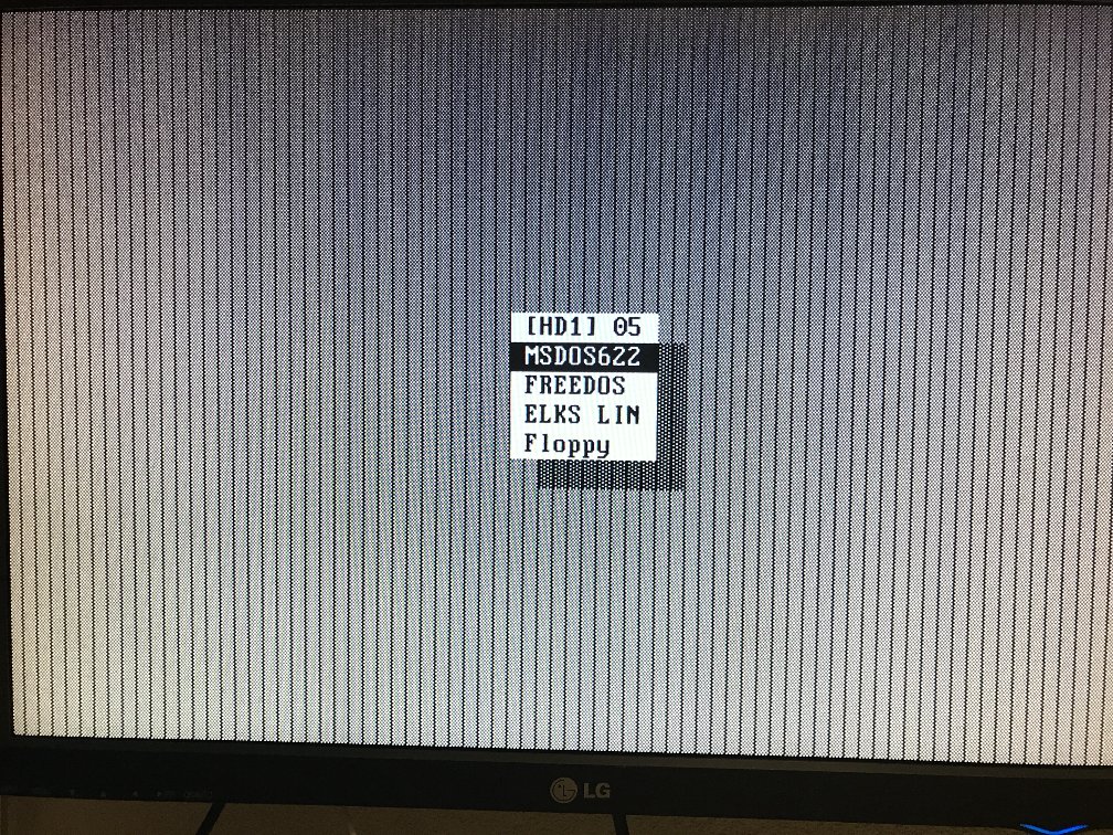
- runs MS-DOS, Windows 3.0, FreeDOS, and ELK linux.
- tested with sound blaster pro 2.0 CT1600 card, including the panasonic CDROM function on the card. Heavy midi loads may experience some lagging due to XT CPU.
- recommended to use the NEC V20 CPU for reduced power draw and higher computing speeds, as well as being compatible with “8088 plus” compiled software that makes use of the NEC V20 enhanced instructions. For example the XT Plus version of the XT-IDE ROM.
- Fixed DMA(4.77MHz), PClock(keyboard)(2.386MHz) and Intel 8253 timer clock(1.193Mhz) frequencies, fully independant of turbo or slow operation of the CPU. DMA clock implemented using a 50% duty cycle custom clock divider of my own design.
- BIOS controlled turbo operation, selectable slow clock speed by CTRL-ALT-numeric minus key on the keyboard. At system power on, the default is turbo speed enabled. Speed can be changed on the fly, I have so far not experienced any crashes due to switching.
- DS12885 Parallel real time clock at ports 070h and 071h, so far I have been unable to properly read the clock, may be cancelled in the future!
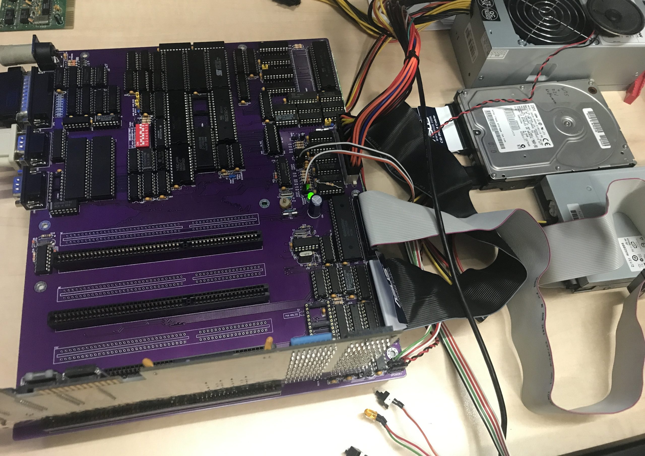
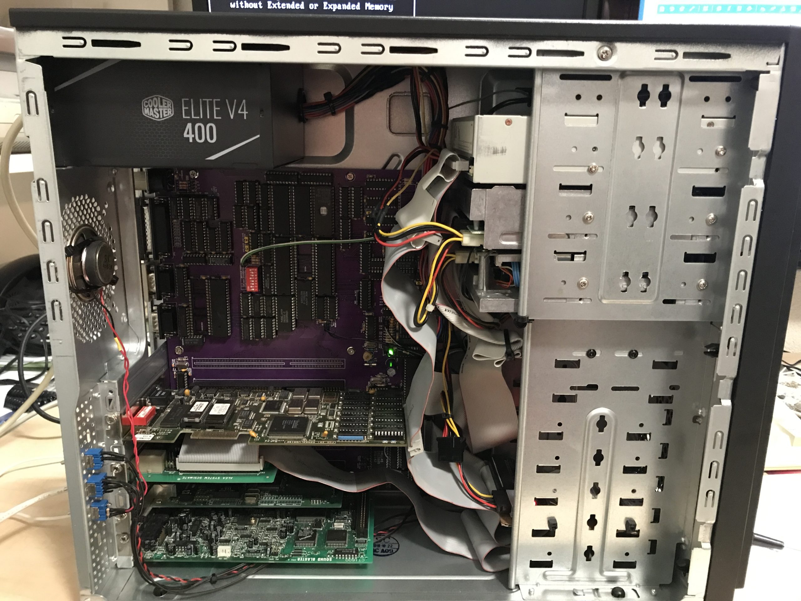
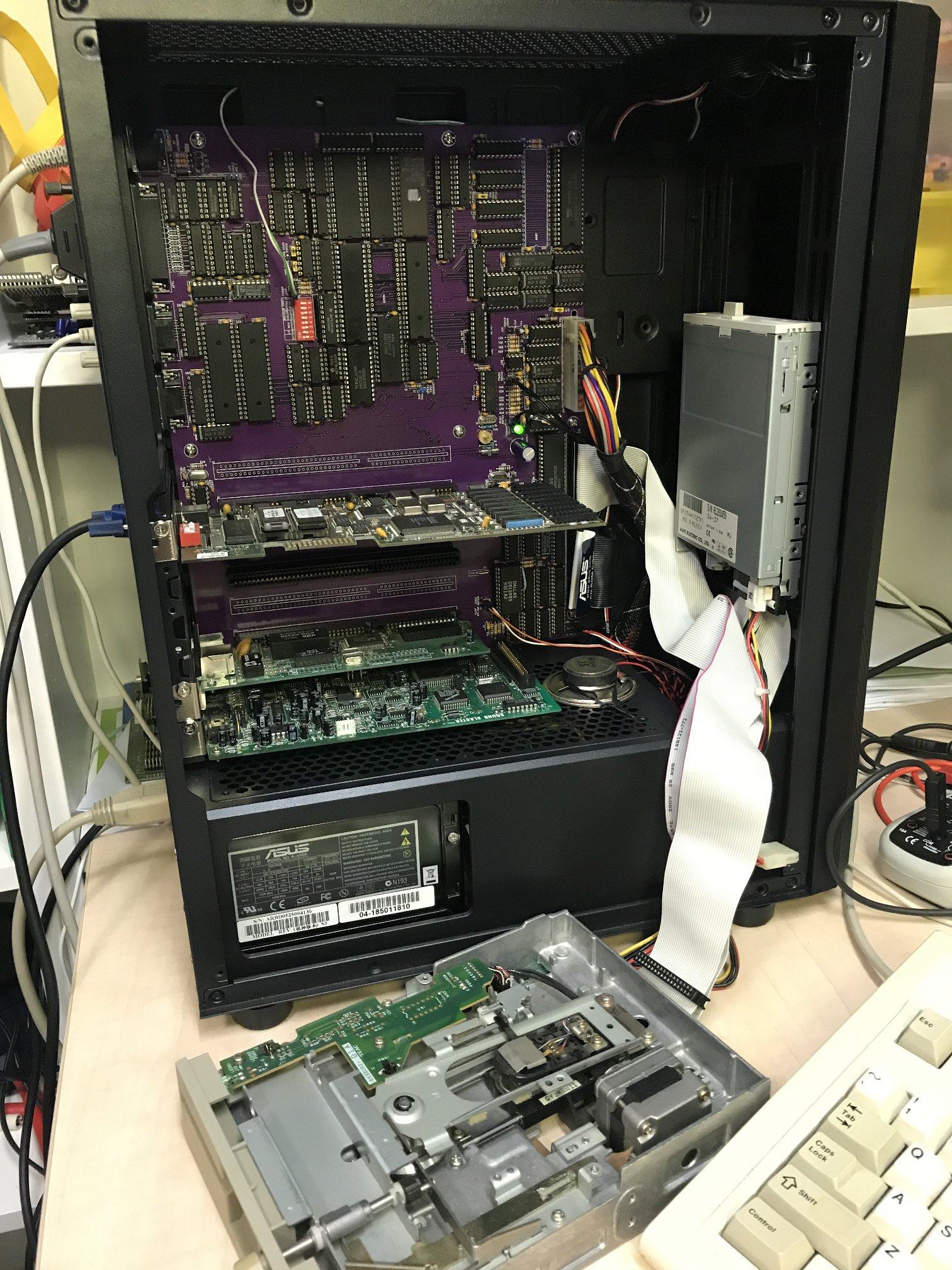
In my process to reach this design, I spent many hours of studying datasheets of ICs, drawing up the missing specification informations, designing and revising various decoding logic, revising bus control circuits, etc, using around 40 pages of A4 written notes and schematic drawings to achieve the best and most compatible logic circuits, while trying to avoid circuits and functions which are not really necessary to implement the design. All these circuits are my own vision to be the most thought-out implementations of logic. After revision upon revision, I finally reached a level of confidence and satisfaction with the resulting design (and end of my patience to review review and review again) to merit a PCB design and prototype production run of 5 PCBs at JLCPCB.
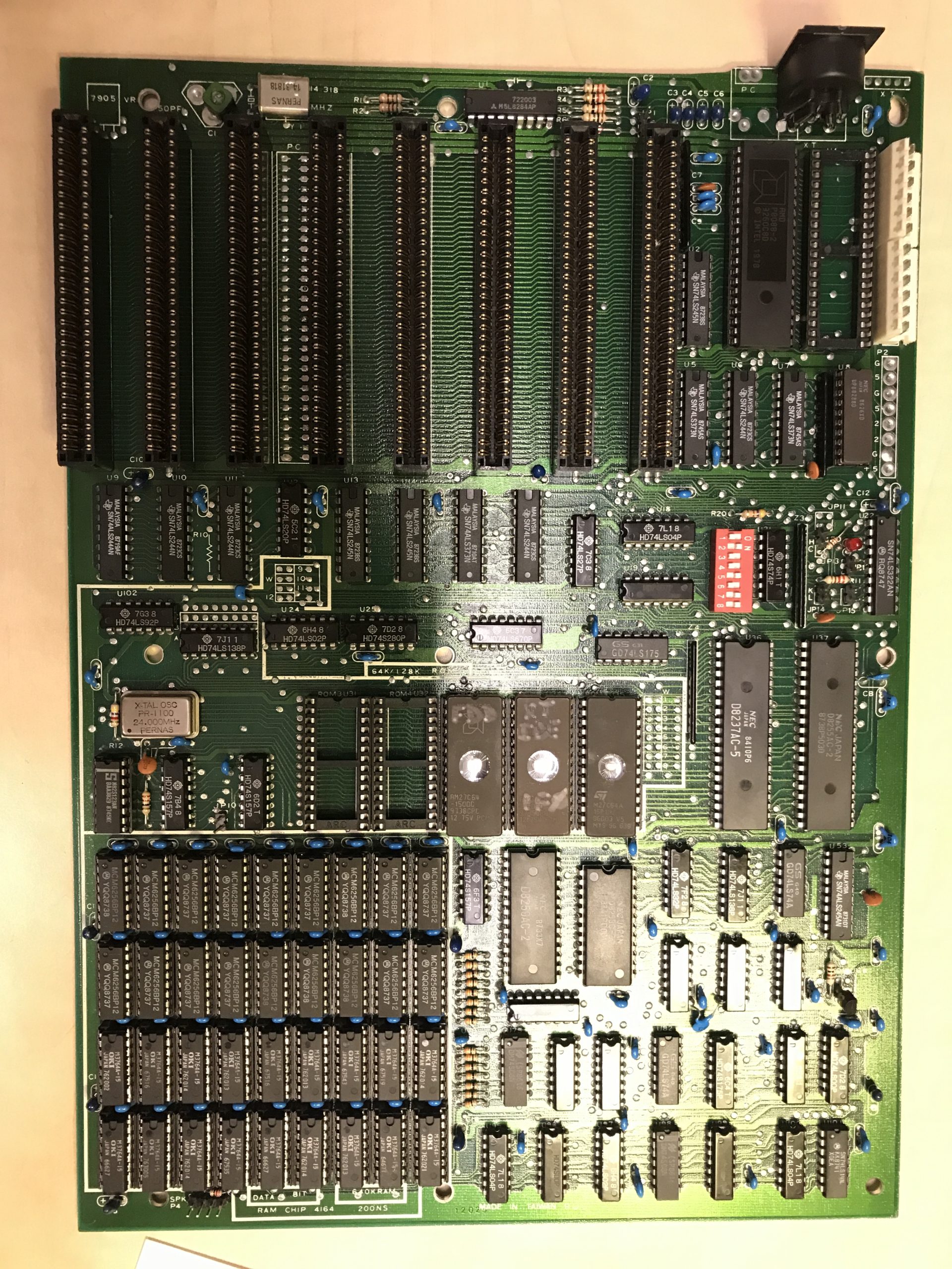
In order to reach this design, during my process, I decided to buy a Taiwanese clone XT mainboard, I washed it, cleaned it and restored it to a proper good condition and stable operation, and have done some provisional testing such as testing the improved XT BIOS, testing some ISA expansion cards etc., just to gain some useful hands-on experience with an XT system. Also I have done some circuit examination of the Turbo/slow CPU operation method used on this mainboard, not liking what I found, and instead deciding to design my own variant of these circuits which uses the fixed DMA, Pclock and Timer controller clock frequencies, needing only to switch the CPU speed, and not the DMA speed as done in other implementations. No switches, no jumpers, only the key combination to switch speed, to my feeling that is more elegant and stable. There is a turbo LED to signal the operation speed.
The DMA processor according to my tests does not seem to need alternate frequencies depending on the CPU speed switching at all. I believe this was more done by clone manufacturers out of practical circuit consideration, enabling a minimal modification of the original IBM circuits. Perhaps many manufacturers in the 1980s were a little conservative and not so prepared to modify many original IBM circuits. I somehow suspected it’s not really necessary to switch all clock frequencies, only the CPU, since the DMA controller operates independantly after the bus is released by the 8088. Later I also found an XT PC design which took a similar approach as my design with fixed frequencies in certain ICs, and I knew it should be safe to go with my own method.
My whole approach taken in this design is definately my attempt to reach a suitable compromise and balance between compatibility and circuit improvement. I just can’t resist to modify certain things to make it more tidy and organised to my own view and preference. There is always a risk involved that complications may occur, but those in my opinion are also opportunities to research, test and learn more and gain some experience. Sometimes you learn additional things from what doesn’t appear to work.
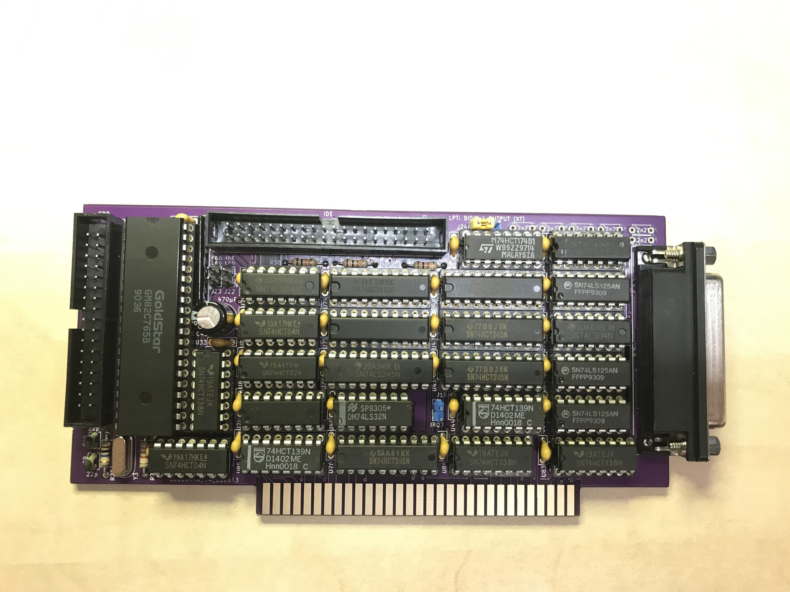
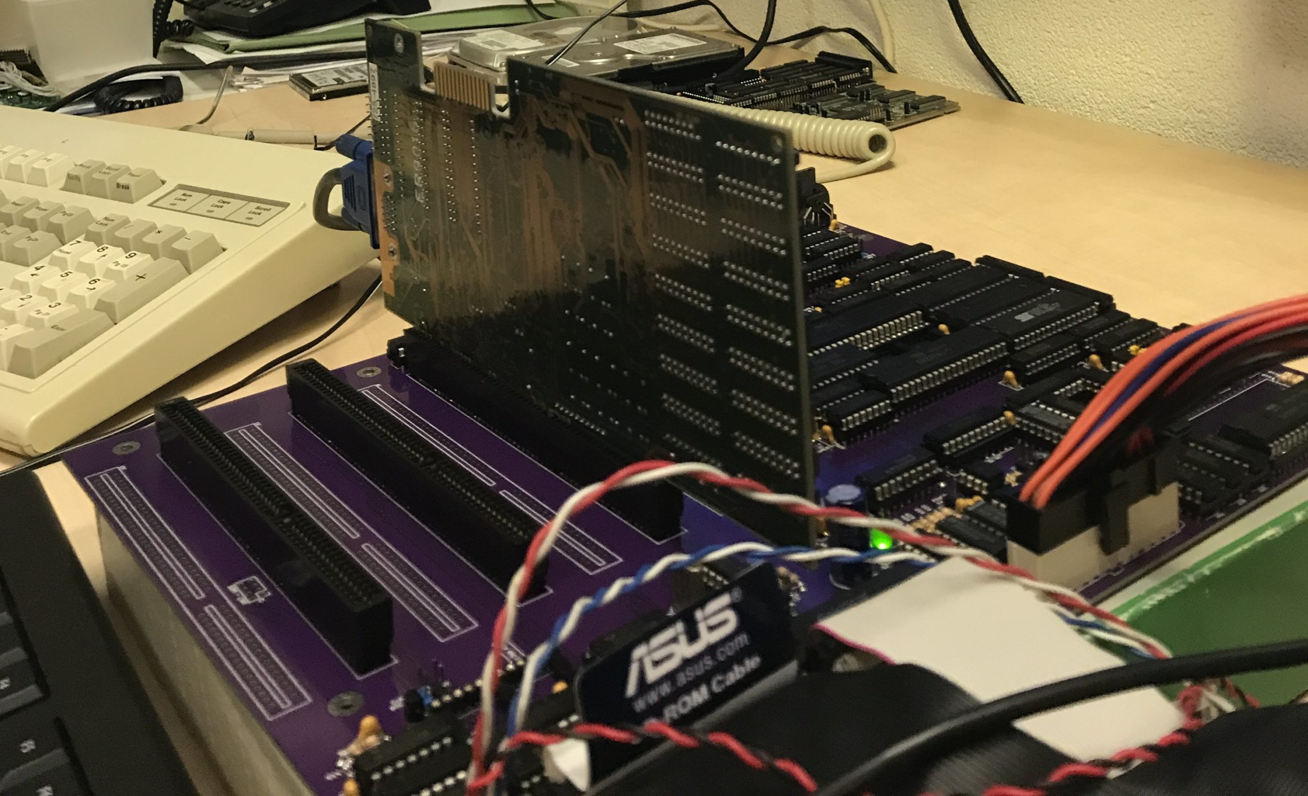
After reviving the above original Taiwanese clone XT mainboard, I have also designed an 8 bit ISA card version of my floppy controller design and my versions of the XT-IDE and an original discrete IBM parallel port recreation. Basically I just adapted the relevant circuits of my mainboard schematics and implemented them on a small compact IO card. The purpose of this card was to test my own unproven IO decoding designs with the Floppy drive controller, parallel port and XT-IDE to ensure they are functional. This process is part of my prototyping process to determine various areas of the mainboard to be known working designs. Definately I can report all three interfaces work well on the card. This card is useful because it provides the floppy drive, harddisk and an LPT port to use for interlnk/intersvr exchange of data for installing all software on the harddisk.
After testing the ISA card I proceeded to assemble and test the ATX XT mainboard. I can report that so far it works really well. All circuits work as intended. For the Trident VGA cards, apparently it’s necessary to connect the /DACK0 refresh pulse to the ISA bus, which I will update in future designs. The V7 video card is better in this respect in my opinion, not being dependant on external refresh pulses from the DMA channel 0, but rather using it’s own refresh logic for the VGA DRAM chips. There you can see the difference in VGA designs. Though the Trident design is much more integrated and reduced, which is also a big advantage of the Trident design.
Timing improvement
During my testing of the mainboard I found that the UART controllers were the most sensitive chips and to be functioning only under certain timing conditions. The occurrences with the UARTs in certain situations were rather strange, for example that a serial mouse is correctly recognised and the mouse program installed the TSR into memory, however the mouse function in the computer was not responding in DOS and windows, howevere after starting the MSD program, suddenly it had a normally functioning mouse control present. Exit into DOS and again no mouse response! Without owning a good scope to check the control timing and bus stability, this behaviour of the UART chips was weird to observe. After further modifications I got the onboard UARTs functioning under all conditions I have tested so far. The solution was using a 47pf capacitor on the RESETDRV line near the outer most bus connector to reduce noise on this signal during it’s inactive state, using a pull-up resistor network on the databus to prevent unknown conditions during tri-state periods, and choosing selectively certain ICs to be LS and HC/HCT types, in order to advance or delay timing in certain circuits. By the way, this technique also proved useful to get the XT-IDE fully stable as well! So there were two problems, one was some tiny noise on the RESETDRV line, the other was timing of the databus. I will be making a full component list to conform with my working prototype.
Now that I have a known good setup, looking back, it was rather an adventure to get things stable and working well, with various unexpected surprises popping up here and there. I can confirm that an XT PC design is definately much more complex and temperamental than a comparable CP/M system! (see my other design)
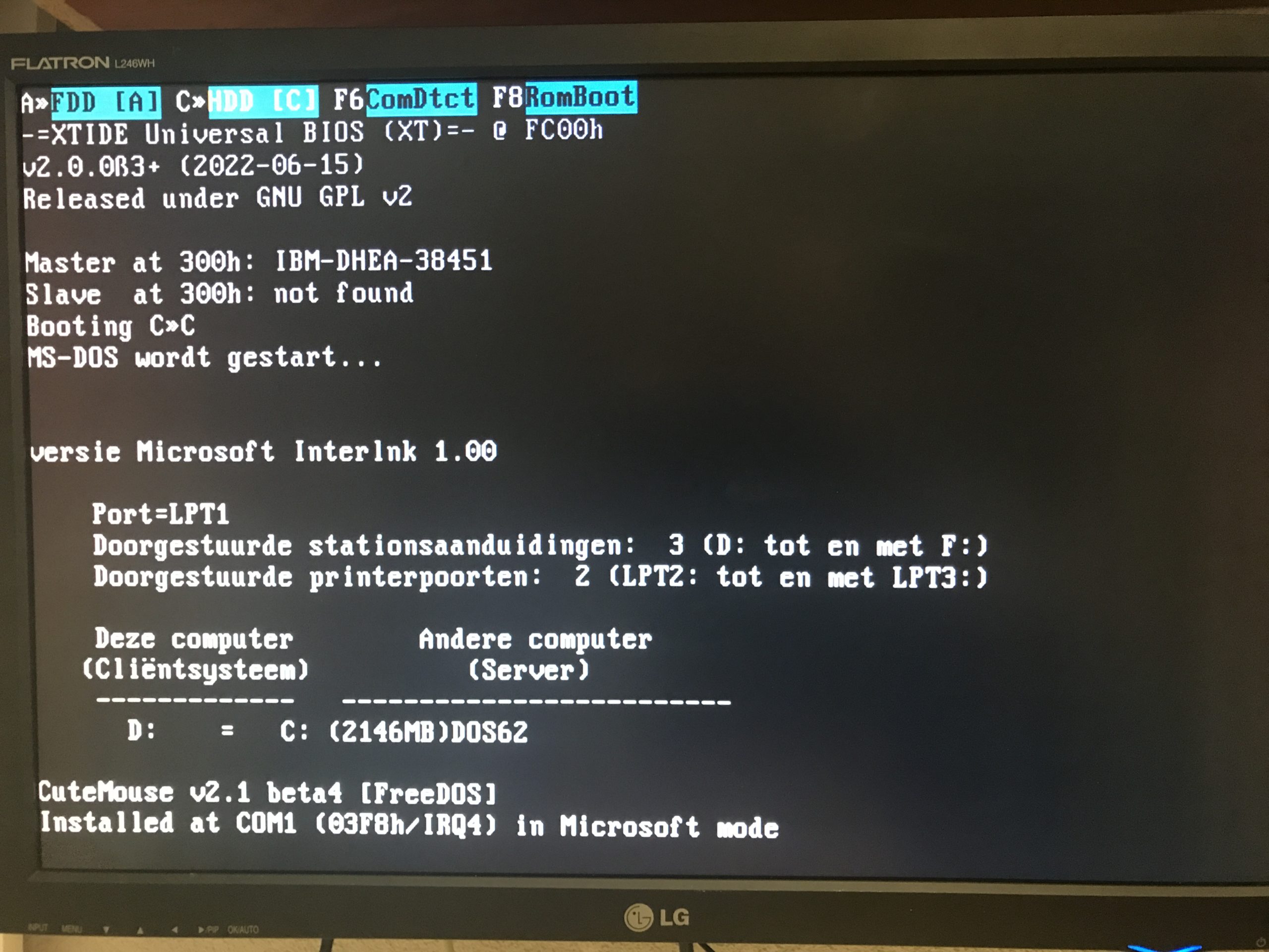
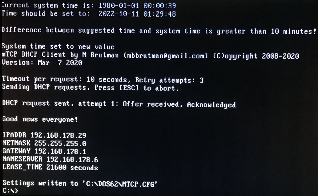
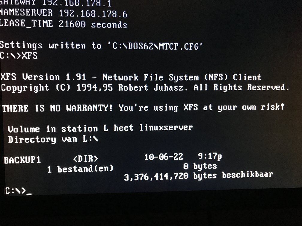
The last things I can report are that a sound blaster pro 2 is fully working, including the panasonic CD-ROM port. Additionally, I have been successful to configure a RTL8019AS ethernet card, and succeeded to synchronize the XT clock, do DNS lookups, read text from websites in the Microweb DOS browser using the mTCP TCP/IP software by Michael Brutman and transfered files to and from my linux server using the NFS protocol package XFS, which is somewhat specific to require lower case characters in all file names on the server side. XFS can offer drives on the network with terabytes of storage space, virtually limitless storage from the perspective of an XT PC. The server reports over 3GB of free NFS space in DOS, but I doubt the storage space would actually be able to run out as this drive on the server has more than 400GB of free space.
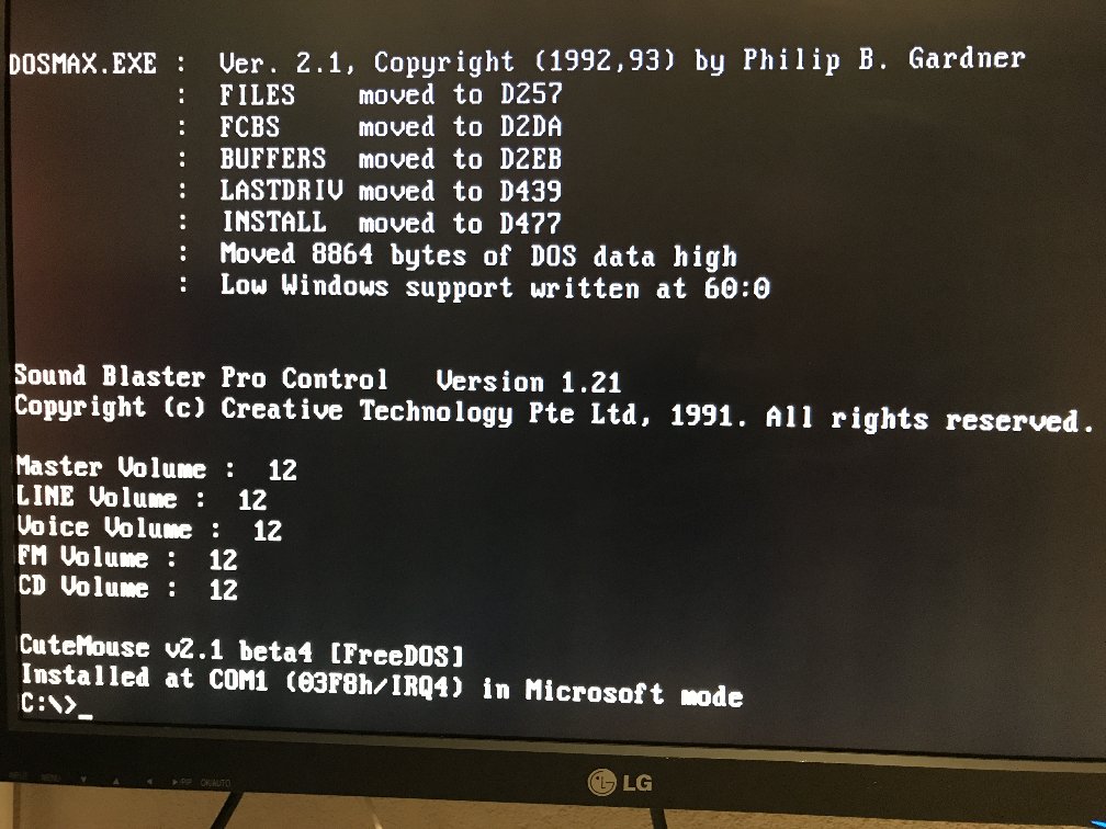
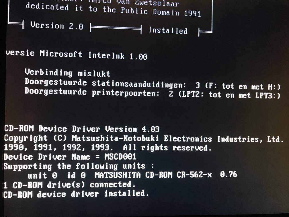
The inherent challenge when trying software on an XT PC is whether or not the software is supporting a 8088 or V20 CPU. For example Freedos contains many programs which require a 80386 CPU. Though I am pleased to find that I can get a lot of useful functionality on this PC. I have since been able to read CDROMs using a Panasonic double speed drive which makes use of CDMKE.SYS, and I was able to play a music CD from the command line. In order to use the Matsushita-Kotobuki CDMKE.SYS driver with a CT1600 soundblaster 2 port, the driver must be loaded by “DEVICEHIGH=C:\DOS62\CDMKE.SYS /SBP:220 /D:MSCD001”.