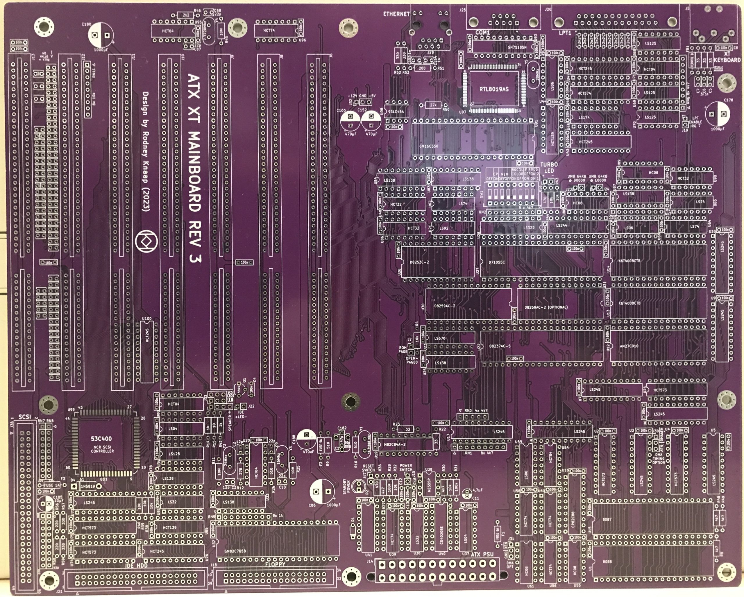
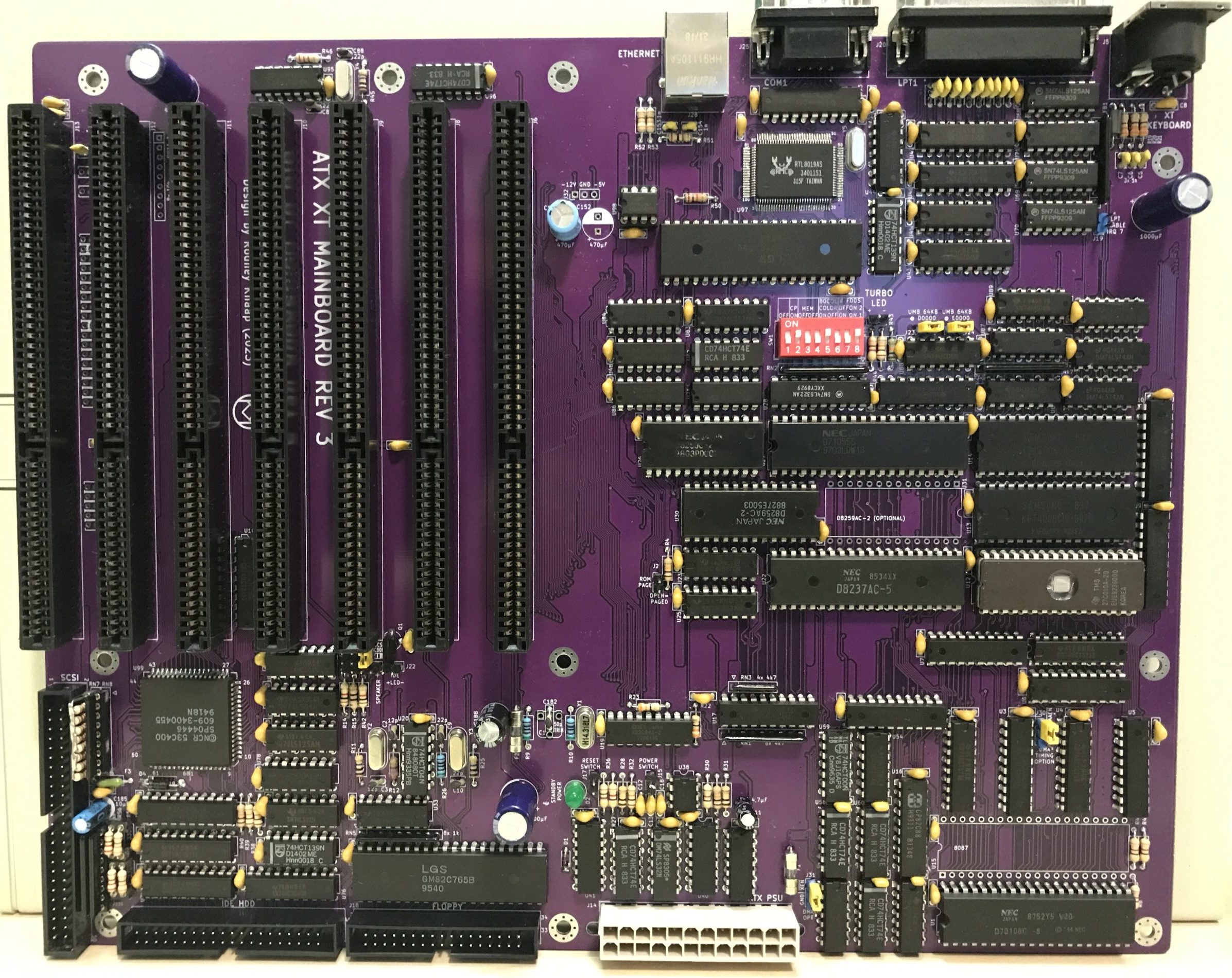
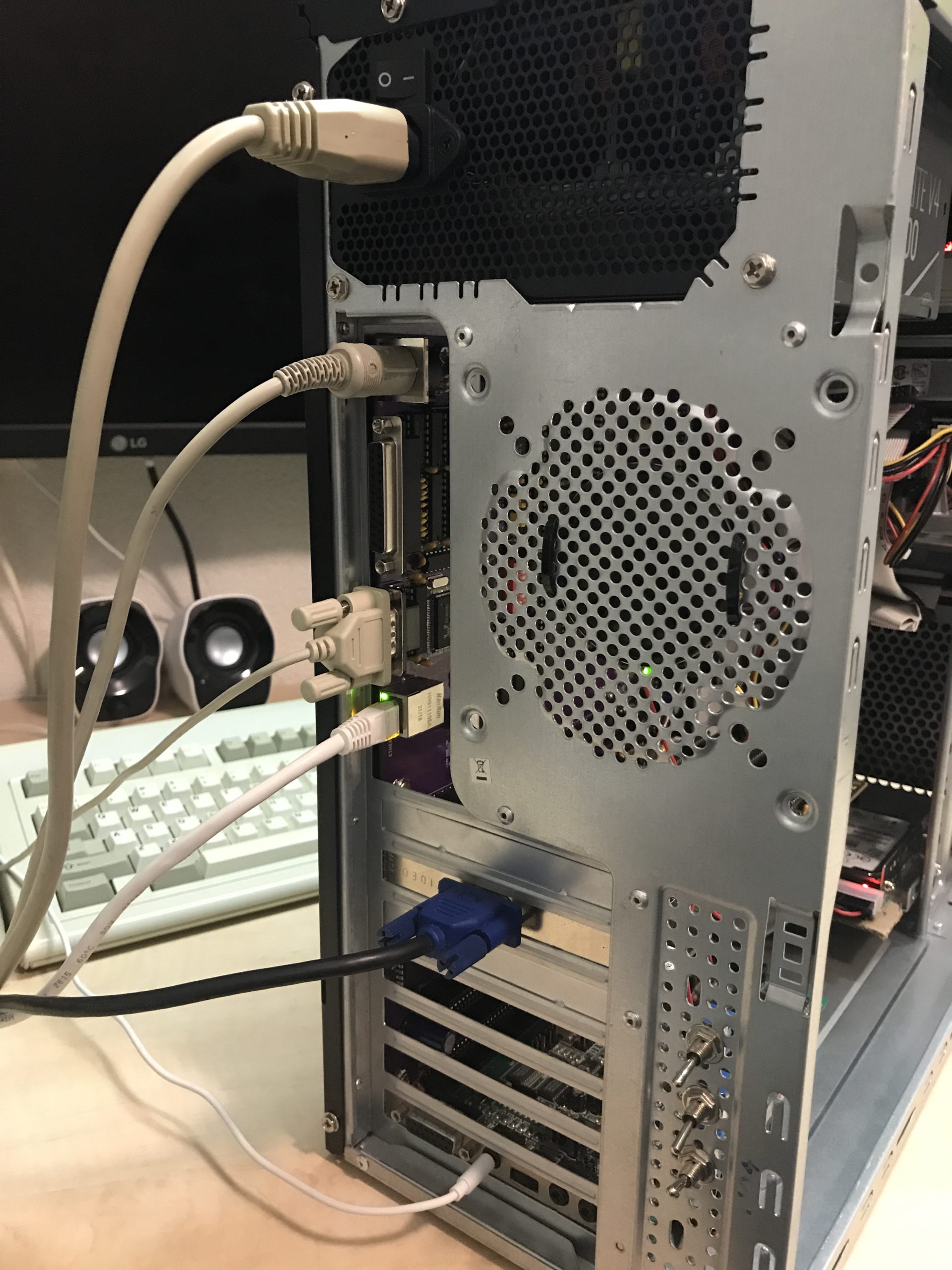
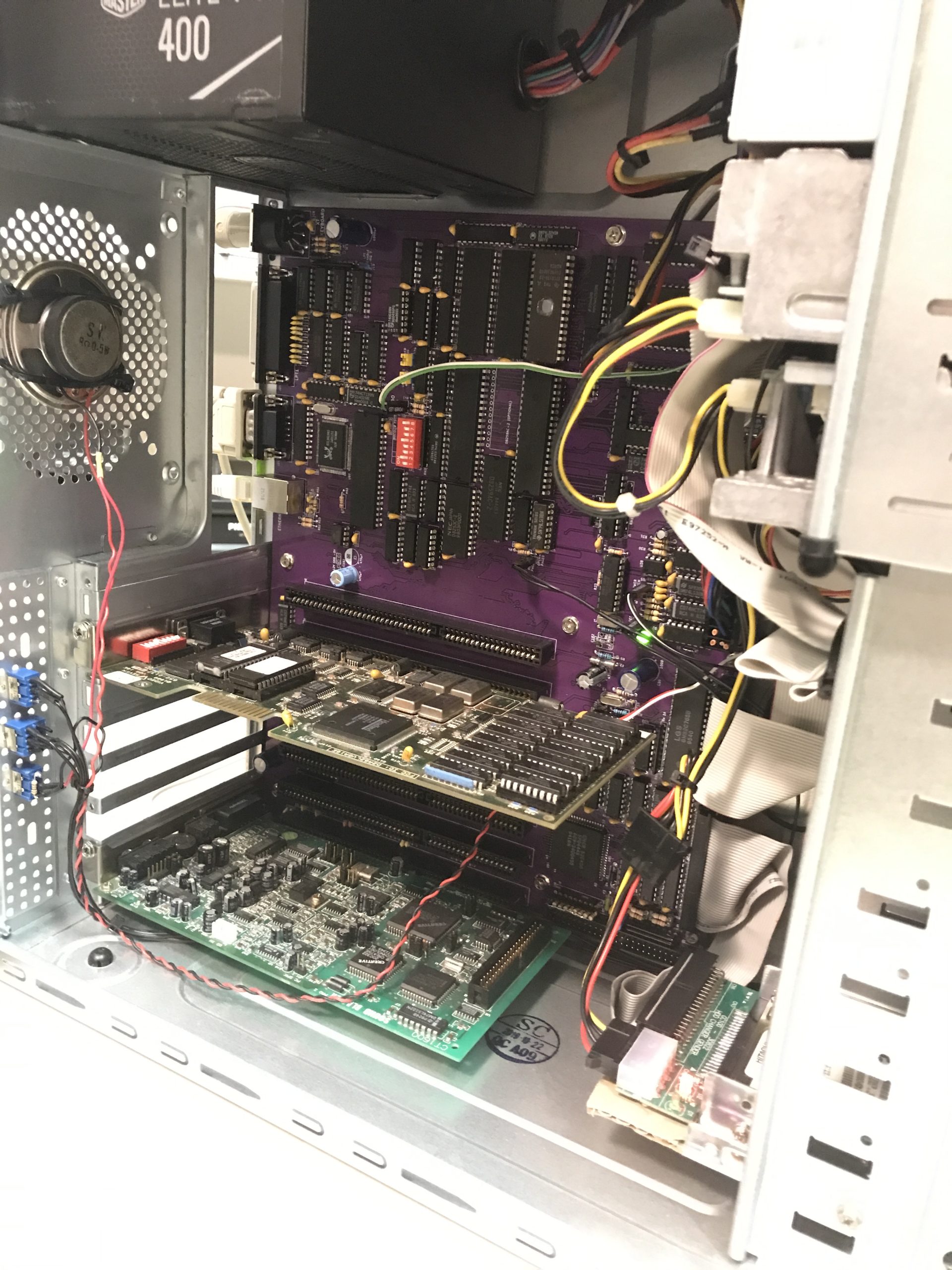
I have made my project fully available for everyone as an open source design.
Introduction
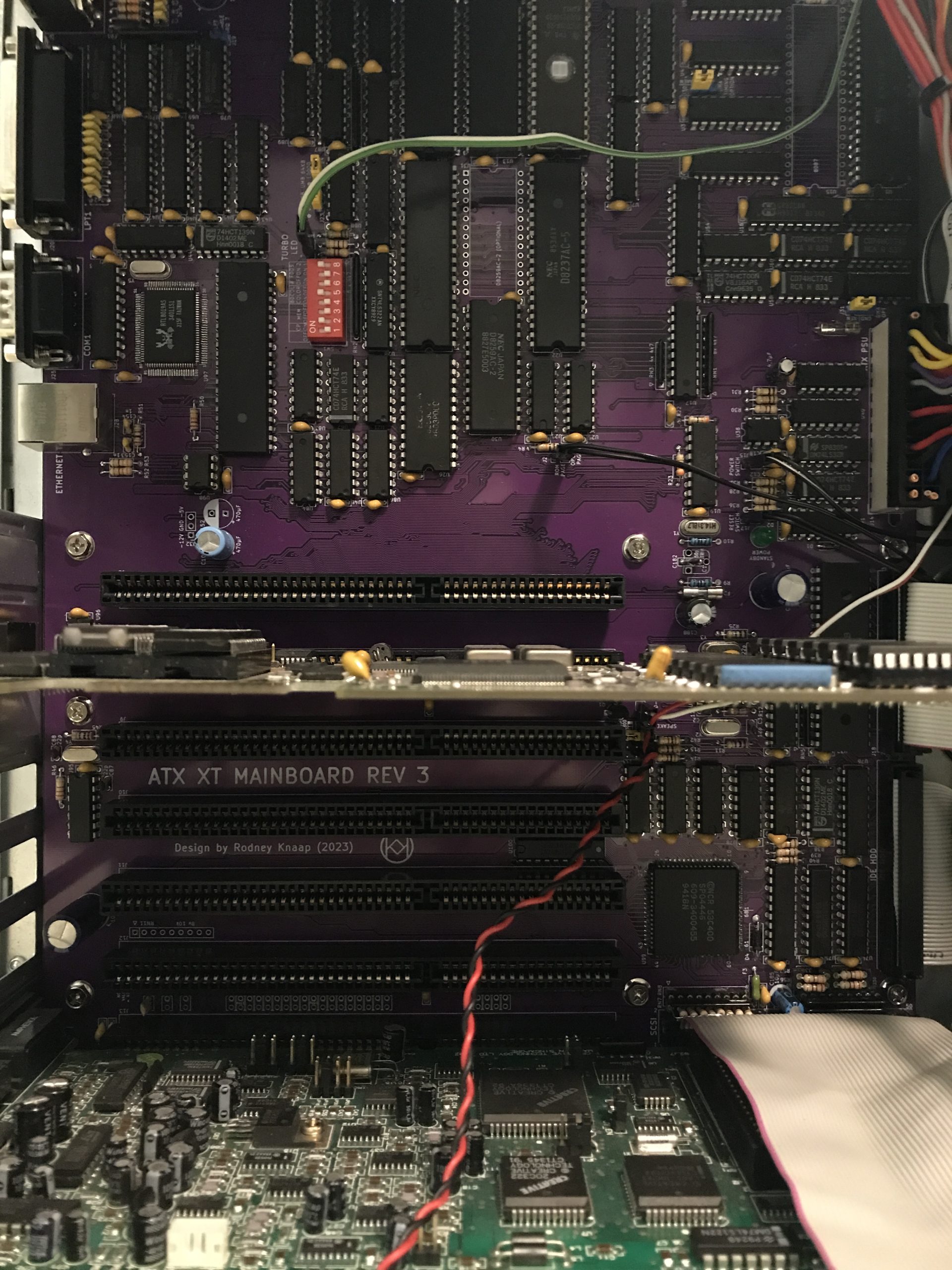
After finding and studying the original IBM XT designs I decided that I would try to design and build my own version of an XT PC, which I found should be possible using "off the shelf" parts, no chipset or custom chips are used on the PC core of the system. I guess you could call this a homebrew design since I made it myself at home, though it was also my goal to produce a professional, fully functional, stable and reliable end result. Basically a modern recreation of the original XT PC system. The only original parts from the 80s era are basically the CPU, DMA controller, bus control, intel clock generator, IRQ controller and timer chip. There are no modern equivalents of course, so I sourced these parts from Chinese chip sellers who sell original recycled parts. I ordered more parts than I needed to make sure I would have at least some functional ICs.
Why would I want to create my own version an XT design? After all, it would not be terribly capable in processing power. There is no practical application for this PC, it's a pure hobby project. However for a combination of several important reasons this is also a meaningful endeavor to me:
- I never owned or operated an XT PC before
- historical and nostalgic reasons
- trying old software
- to experience what the limits of an XT PC system would be
- to gain more insight and understanding into the foundation of PC design and start of the industry PC standard
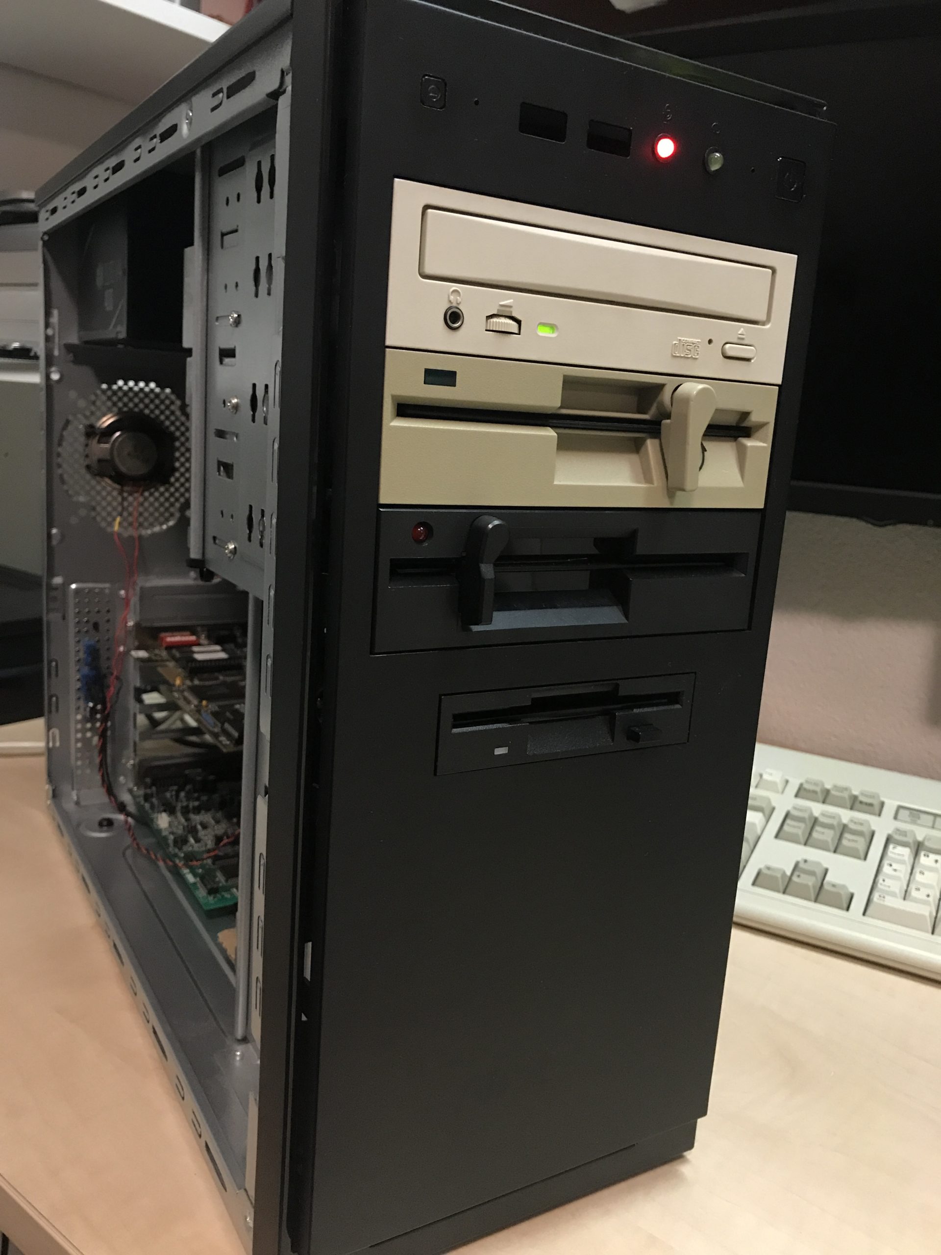
- to be able to easily mount an XT mainboard in any full size ATX PC case
After extensive verification of my CAD schematic, I decided to make a few changes to the original IBM circuits which I felt would be an improvement.
- merging some buffer ICs
- changing the dip switch circuit
- adding "Turbo" CPU clock and control logic
- fixing the DMA clock to 4,77 Mhz 50% duty cycle with my own clock divider circuits
- deriving all XT device clocks (DMA, Timer, Keyboard) from 14,31818 Mhz fixed OSC clock on XT oscillator
- removing the refresh and multiplexing logic of the DRAMs and replacing the entire RAM range with 1MB of SRAM memory chips, using jumpers to enable the D and E blocks of upper memory RAM, supporting to load drivers in UMB areas and free up conventional RAM memory
- double ROM memory space(128K) in a single ROM chip with a jumper or switch to select the active page
- changing various logic on the CPU/DMA WAIT control and CPU/DMA switching of the bus
- adding the 16 bit extension part on the ISA bus connectors, mostly to accommodate larger adapter cards fully into a slot
I spent some work into double checking all circuits and partially developed certain circuits using paper notes. Totally I drafted 38 pages of A4 size design notes and logic tables to verify and reach the first revision stage XT design, which functioned right away when first powering it up.
Integrated design:
When looking at PCs there are usually a number of typical devices you would wish to include in your PC computer, such as:
- Keyboard interface (real and original XT keyboard function)
- Serial port for mouse functions
- Parallel port for printing and interlink connection to other PCs
- HD floppy drive interface
- IDE harddisk interface(compatible to work with XT-IDE BIOS)
- LAN adapter
- ATX power control and (power-on) reset logic
- SCSI adapter supported by existing DOS drivers
- simplified power on and reset circuits
For the LAN adapter I decided to choose the widely used Realtek RTL8019AS chip. This chip contains all decoding logic and uses a serial EEPROM for part of the configuration. Though I would have preferred to simply add the decoding to my own logic circuits, since it's included inside the Realtek chip, I used the Realtek decoding logic.
The SCSI adapter required some more experimenting and testing, since I needed a working device driver for implementing the SCSI ASPI control and another two drivers for adding a SCSI harddisk volume to DOS and for supporting a SCSI CD-ROM drive. After extensive testing with the Rev 2 prototype of this mainboard using a Zilog 5380 clone chip, I decided to choose the NCR 53C400 chip instead. The main reason is simplicity of design, despite the disadvantage of the chip being physically larger in size. The 5380, though setting a standard, is unfortunately not a straightforwardly used chip on adapter cards. None I have seen used the straightforward connection. Except one, but that card only offers windows 95 device drivers. Since this XT PC is a low performance 8-bit 8088 system to begin with, and as I am integrating the SCSI on my mainboard for which I want to allocate as little board space as possible, I finally chose the NCR 53C400. This chip provides a compact SCSI interface which is known to be correctly supported by DOS drivers on an 8-bit XT PC. The drivers I used are flexible, stable, small and load quickly on an XT with a 8088 CPU. (I actually tested with a NEC V20) I have tested this SCSI chip with several harddisks and SCSI CD-ROM drives and the results were very satisfactory.
Since my XT doesn't include USB capability, the SCSI interface is a really useful alternative for file copy and transfer to the PC using an external SCSI harddisk. This was the main reason for me to want to include SCSI on this mainboard.
The ATX power on and reset logic I first made included a few extra circuits such as power good verification and auto-shutdown circuits, however I found later that under certain conditions these circuits proved to be a bit unreliable in not always powering on. After several tries to solve this, I decided it would be better to remove the auto-shutdown parts and simply implement power on logic and reset control and timing circuits. On this 3rd revision things work under all conditions of external connections to the PC which to me now is more important than elaborate power-good checking.
Basically, everything I would want to have is included on this integrated design, except:
- VGA adapter
- Sound card
I don't want to include these on the mainboard because these cards are really something one would want to add separately according to preference and experience while trying the computer out. All the VGA cards I have here which support 8 bit BIOS operation are fully functional on this mainboard design. Maybe later if I would decide to make a fully integrated PC in a so-called "pizza box" format, I may choose to integrate the VGA and sound as well to reduce the total size of the PCBs used. I may even entirely leave out the expansion bus in that case, or just keep one slot for optional testing and diagnostic purposes. The pizza box case would house the entire PC on one PCB in the bottom of the case and above it only house a power supply and the disk/disc drives.
Functionality of the XT PC today
This XT PC is not capable of much if you only regard the processing power or the fact that it's an 8 bit PC. On the other hand, slow or not, the XT PC is able to perform more tasks than you would expect. It's all a matter of perspective, how you look at the system. This PC is capable of managing and copying gigabytes of disk storage, it can run DOS, Windows 3.0, a simple form of linux(ELKS), play music, create and print text files, display photos in 256 colors, and play various games. The system can read CD-ROM media and copy from them. Though slow, it is fun to explore the limits of this simple 8 bit system and sometimes it can surprise you to be able to do more than expected. It's fun to use DOS and remember how mainstream computing was back in the 80s and 90s. What I also love is the reliability of this system after I completed it. The "old" components I used are a tribute to the quality of the 80s era chips, they are real survivors, probably the manufacturers are still proud of what they accomplished when they still see their chips alive and working today.
Some people like the original IBM XT systems, which I agree have their own charm, they look nice and cool. However when using them you will likely encounter problems and limitations very soon. That's why I personally like a more expanded system more than original XTs, simply because we do have this technology available such as larger IDE drives, SCSI, VGA, CDROM, etc. So why keep the limitations and problems? I enjoy the experience of making a system live up to its full potential.
When you see what people have recently created for XT PCs you can see that they are still popular amongst enthousiasts. Not for the processing power but for the historical value of the XT computer. There are various communities where you can find enthousiastic classic computing fans. Often they are people who experienced those days in the 80s and 90s. Though at the time I never saw a PC until the late 80s myself. The first PC I used was actually a 80286 system.
Using the LAN connection this XT PC can accurately set the date and time via an NTP server, which I have included into my startup. I was able to use NFS to some degree, with mixed results due to software bugs in the NFS client software on the XT side. The XT can view web pages on a text based browser, it is possible to read the website text content.
About the SCSI bus, I will make a custom cable to run from the slot bracket in the back to the SCSI bus on the mainboard, and running it through to the top to connect the CD-ROM drive. I will probably make a terminator which can plug into the rear 25 pin SCSI connection at times when I am not using an external SCSI harddisk. That way, the termination on the mainboard will not be necessary anymore.
Delicate DMA timing
I experienced some difficulty with the 8237 DMA controller at various stages of my 3 design revisions of this XT mainboard. This time when I found the same occurance, I decided to dive into the problem in more depth to determine the reasons why I was observing the problems. The DMA handover and bus control is done by various logic circuits, where I found the difference in operation was due to subtle timing differences. Especially the timing on the DMA address latch outputs turned out to be critical in the DMA process.
Timing problem finally resolved
I revisited the DMA timing several times to see how I can improve the timing beyond the margins which allows the XT to function properly with typical DMA controllers found in more recent XTs and AT PCs with separate 8237s in them.
When examining my Taiwanese clone turbo XT reference mainboard another time, I noticed that some of the TTL ICs were not of the LS type but they were ALS type instead. This was a big clue to support what I previously suspected to be the cause. Which is TTL IC propagation delay times. The 74ALS and 74F logic families are somewhat faster to propagate the logic switch on their inputs to their outputs. So this can come in handy on my XT as well. When I checked the ICs in the clone XT mainboard I confirmed that those ALS ICs were indeed involved with the DMA system in this XT. Additionally I noticed another thing, the Taiwanese designers also replaced the DRAM delay IC with normal logic somehow. I have not checked this in detail but this is indeed remarkably different from the original XT. Creating a timing delay is of course possible in several ways depending on the delay needed, the margins that need to be kept and a possible allignment on clock transitions which is also ideal to be able to time signals.
I checked my schematic and decided to replace a selection of DMA related ICs with ALS and F types. My preference of glue logic was to use F types there because I saw in some datasheets that these are really fast.
I replaced the following ICs:
U24 - 74ALS573 (no F type available at the moment)
U55 - 74F08
U58 - 74F74
U59 - 74F00
U60 - 74F74
After this I have done some testing, and indeed it was quickly apparent that all the NEC 8237AC-5 DMA controllers I have (about 10) function perfectly now. Additionally, I found that formatting a diskette now already starts stepping the floppy drive on the diskette tracks even before the command line is updated to show the percentages. So DMA is now working faster and better than ever.
This final fix now definitively concludes all the issues I came across in development and testing and I consider the design now completely bugfixed. I will update the partslist in my GitHub page accordingly in case anyone wants to build this project.
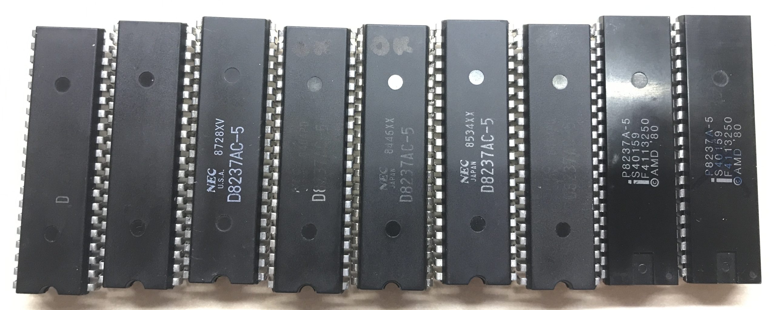
In the photo above you can see the different DMA controllers I have tested. I received 10 DMA controllers from China, most are NEC branded ICs, two of them are from Intel. It's a funny fact that the 8237 DMA controller is actually made by Intel in license from AMD. So the design of the industry standard setting DMA controller is made by AMD. Recently I saw one made by Intel bearing the copyright mark by AMD. Which is a funny reversal.
Of the above photo, all 7 NEC DMA controllers work perfectly with my design. The Intels are problematic and one of them is even defective. I recommend using a more modern DMA controller chip which has the normal typical plastic package as seen in the photo above.
Final remarks / conclusions
This 3rd revision design is now fully tested so I consider this project finished. At the moment I don't see any big reason to produce a revision 4 PCB.
It was a great experience to test and use this PC, it has turned out to be a very comfortable and functional system with comforts of use such as for example easy power control using the ATX power supply with a modern front panel switch, unlike the AT systems of the era which use bulky mains power switches, sometimes located at the back of the case. I use a Cherry G80-1000 XT/AT keyboard which is really a pleasure to type on.
Next Project: 80286 Turbo AT ATX PC design
Next in this series of PC mainboard design projects is the 80286 Turbo AT ATX PC project.
I have finally taken the step to work on this project, I have found some suitable reference example mainboards for testing and evaluation. The work is looking very promising and I am getting more and more enthousiastic the more I dive into the schematics of the IBM 5170. As far as I'm concerned, time permitting, the AT project will become a reality!
I created a page here: continue reading on my new project page at this website...

