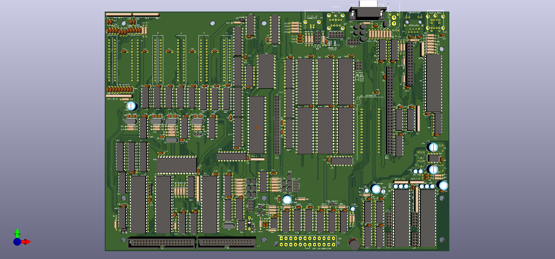
I have done various PCB design and building projects since the late 90's. Usually those projects were Z80 based. I started with the ZX80 and ZX97 Lite, and continued with the ZX81 Issue 4. With every new project I tried to raise the design level. I did some DIP projects and also some SMD ones after doing a lot of SMD soldering for my work.
I have always had the wish to build up a more complete system which has the capabilities similar to a classic PC. When I found some projects based on the RC2014 retrobrew Z80 system (invented by Spencer Owen), and especially after seeing the very excellent BIOS and bankswitching system project called ROMWBW, which was created and is being maintained by Wayne Warthen, I knew that I had found something special that would be a really feature rich system to build and try to expand further!
I decided to build up my own Z80 system, inspired by the ideas I have seen on various pages made by users(Karl Brokstad, Spencer Owen, Scott Baker, J.B. Langston, Marco Maccaferri) who were building RC2014 systems with their own hardware additions and modifications. I decided to design some basic circuits from KiCad schematics and logically combine some things. I spent some time testing a couple of hand wired PCBs and came to the conclusion that this system with the current expandibility would really deserve and benefit from a mainboard PCB design.
This mainboard serves to set a known functional hardware base from which I can develop both in hardware and software. The mainboard is intended as a through-hole only project, making it easier to solder. There is one exception, a 8 pin USB to UART chip, which is however purely optional and can be replaced by a small plug in PCB which plugs into the included header. Additionally, an ethernet controller is a 100pin SMD chip, which should be soldered to an adapter board, yet to be designed.
One thing which I concluded most notably after my prototype testing is that amongst the many designs supported by drivers in ROMWBW, one thing was especially missing, a fast graphics adapter which could connect to a PC monitor and display in higher resolutions. So this is definately on my wish list to develop one! I am doing the research for this plan now.
Long story short: I redesigned the IO decoder circuits, integrated some buffering, split the Z80 bus in three sections:
- Memory bus (memory access only)
- I/O bus (I/O devices only)
- Expansion bus (an extension of the I/O bus which only becomes active if an "offboard" expansion device responds to the IO address it is designed on.
I tested with various circuits to power on and off an industry standard ATX power supply, and designed a reset circuit. These formed the basis of a mainboard design which has the following functions:
- Z80 CPU
- Z80 CPU expansion connector (replacing Z80 or take control of system with other CPU)
- one flash ROM memory chip of 512kb according to ROMWBW bankswitching system
- 6 SRAM memory chips of 512kb each, one of which can be jumpered to become an extra flash ROM if needed
- GPU slot which contains access to shared RAM of 512 kb and two latched I/O handshake ports
- 6 device expansion card edge slots (device I/O only)
- PPIDE harddisk controller port
- RCWDC floppy drive bus
- ACIA serial port for connection to a IBM PC via standard A-B usb cable
- TMS9918 CRT controller NTSC composite output
- dual YM2149 mixed to 3,5mm line output connector (trimmer adjustable volume)
- dual SN76489 sound chip, mixed to same 3,5mm line output connector (trimmer adjustable volume)
- cassette tape output and input similar to Sinclair home computers
- VT82C42 PS/2 keyboard and mouse ports
- DS1302 realtime clock chip with offboard battery connection header
- RTL8019AS ethernet interface (using a small SMD-to-pins plug in PCB)
- ATX power supply control to standard 24 connection ATX power connector (including soft-off, made with conventional logic ICs)
- power-on reset circuit with clock based timing (also with conventional logic chips)
- 18 LED outputs for signalling various system functions, on 3 small headers, custom LED front panel is planned
Not everything on the list is supported by software drivers yet:
- the cassette tape loader software needs to be written (great starter project!)
- PS/2 mouse function is not made yet
- Realtek ethernet connection software needs to be developed, though I have read that there is NE2000 code which might be compatible, and Realtek does offer many support files which may contain helpful information!
- dual YM sound, I am not sure if there is some software which could do it.
Hardware design for the GPU controller PCB is pending, I am currently doing research to determine what solution would offer the best functionality. I am looking at "bare metal" programming the ARM processor on a Raspberry Pi zero board, and also I am considering an FPGA board with the ARM CPU included as a soft processor core.
The problem when looking into programming the Broadcom 2835 on the Raspberry Pi Zero is that this Broadcom chip is basically made to form the core of a mobile phone, and is much more complex than a mere ARM processor. In order to use it purely as a processor and redesignate it to completely new functions, I will need to determine the right way to do it, and how to make use of the GPIO pins in order to interface to the SRAM and handshaking latch circuits shared with the Z80, and how to output the VGA data to a screen. The big advantage of the Broadcom chip however is the very low cost price and amount of processing power and coupled memory space which can become available when using this chip.
There is a GPU slot present on the mainboard which passes the VGA signals through to the VGA connector already present in the IO Shield area.
The mainboard is ordered from a Chinese PCB manufactorer last weekend and already en route to my home, I am expecting it to clear customs in Germany at some time, after which I hope to have the first boards for testing!
I have implemented full buffering on the buses, and redesigned the IO decoders in a universal method. I still will need to test if with all these circuits the timing will be sufficient! I will update this page as soon as I have more news about this.
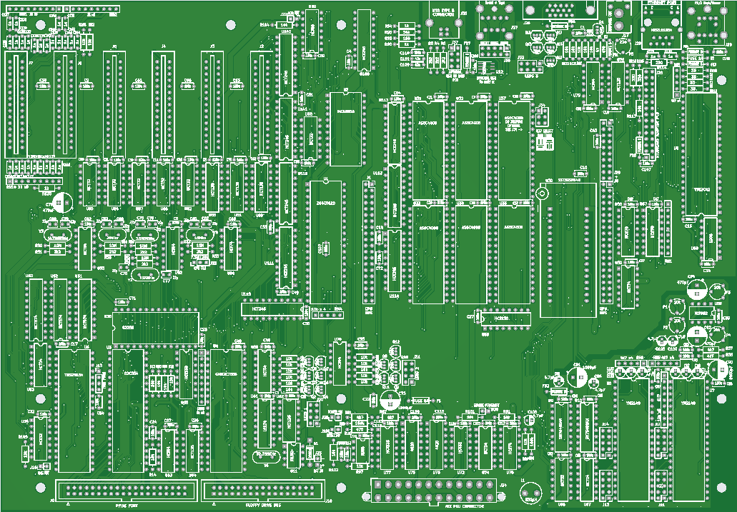
Update: Prototype mainboard
13-2-2022
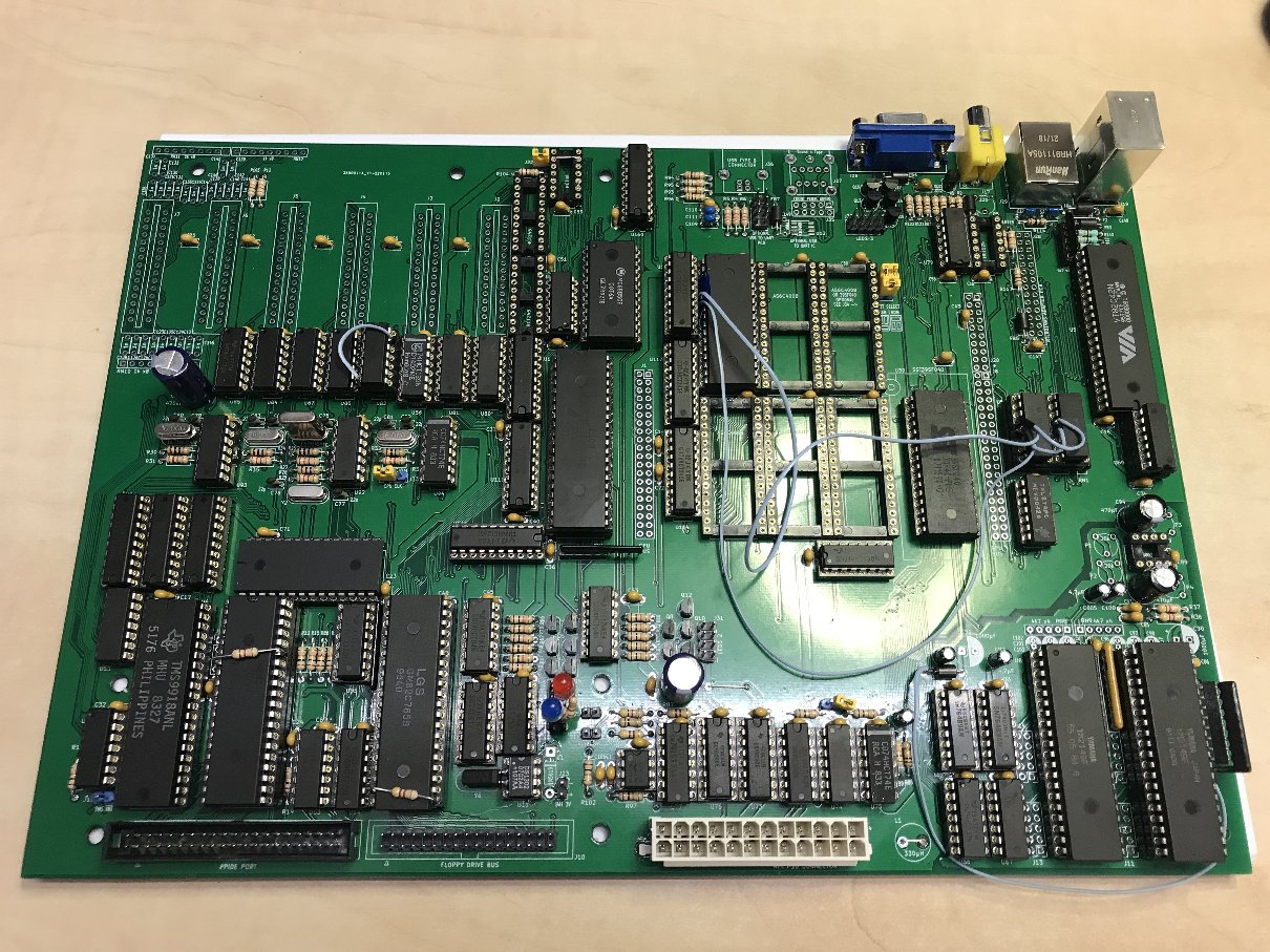
I have received the manufactured mainboard PCBs from JLCPCB (a big recommendation from me!) and built one up.
During my test work I have found some issues, as I expected. The problems were easily solved with some small modifications.
The first revision mainboard contained following parts:
- ROMWBW
- PPIDE
- RCWDC floppy controller
- ACIA
- YM sound on one chip, I need to see if any software is available to test both YMs for a total of 6 channels
- DS1302 realtime clock
- ATX power supply control
- power-on reset circuits
- PS/2 keyboard interface
- TMS video output
- USB to serial console connection for CP/M
Second Revision Mainboard
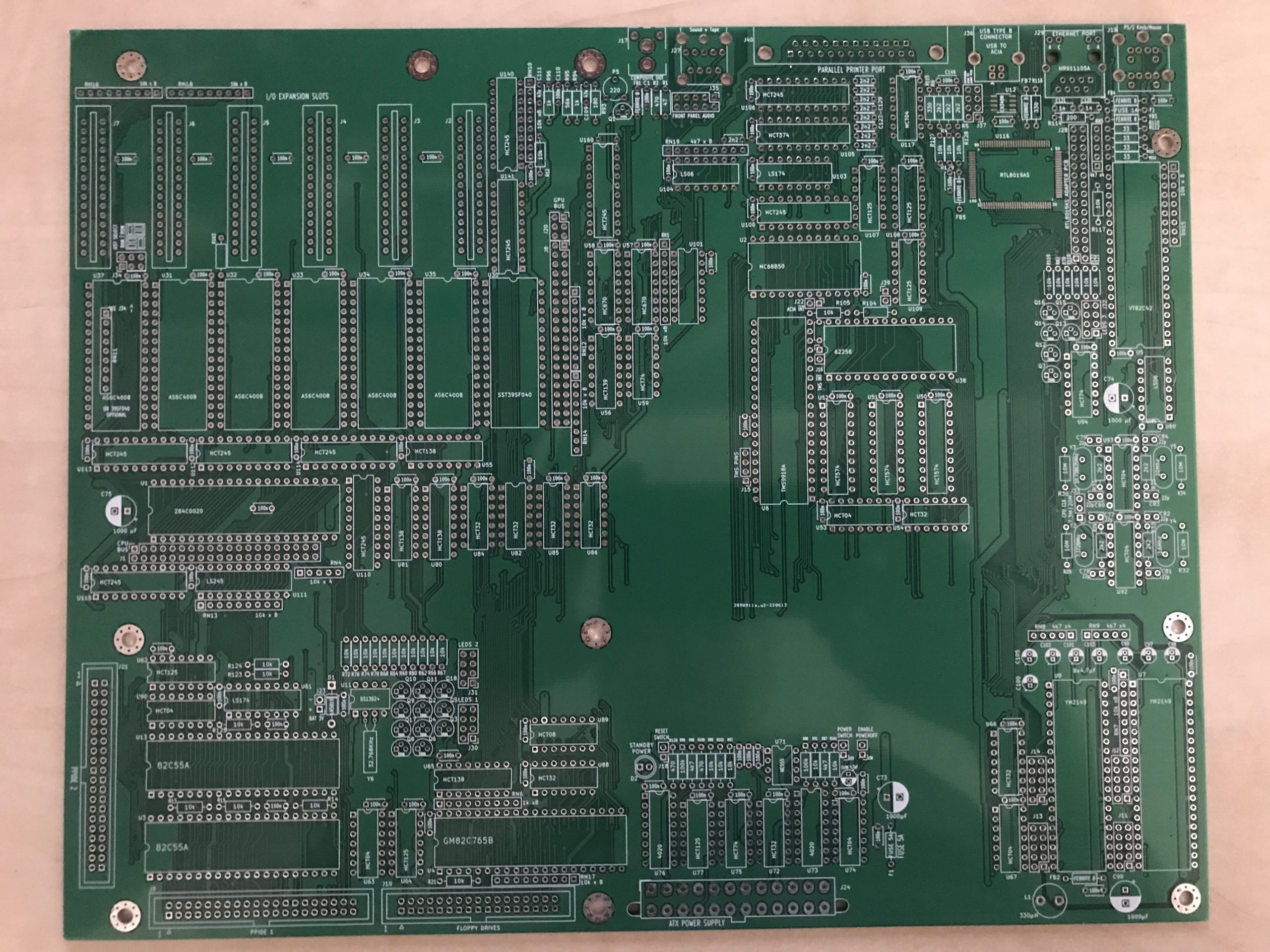
After completing the first revision mainboard, I quickly moved on to the second revision.
- two PPIDE interfaces instead of one
- removed the noisy SN76489 chips
- added onboard RTL8019AS footprint to optionally fully assemble the LAN adapter onboard
- added discrete centronics style parallel port interface for printing or other purposes
- changed the power circuits on onboard USB serial console interface to power the interface chip from the USB connected PC to avoid serial interface disappearing on PC during power cycles of the Z80 system
The second revision mainboard is fully tested and functional. I have started to write documentation and disclaimers etc, however this is extremely time consuming and I have been working on other projects which also near completion. I do plan to finish this work but I am not sure when I will find enough time to complete it.
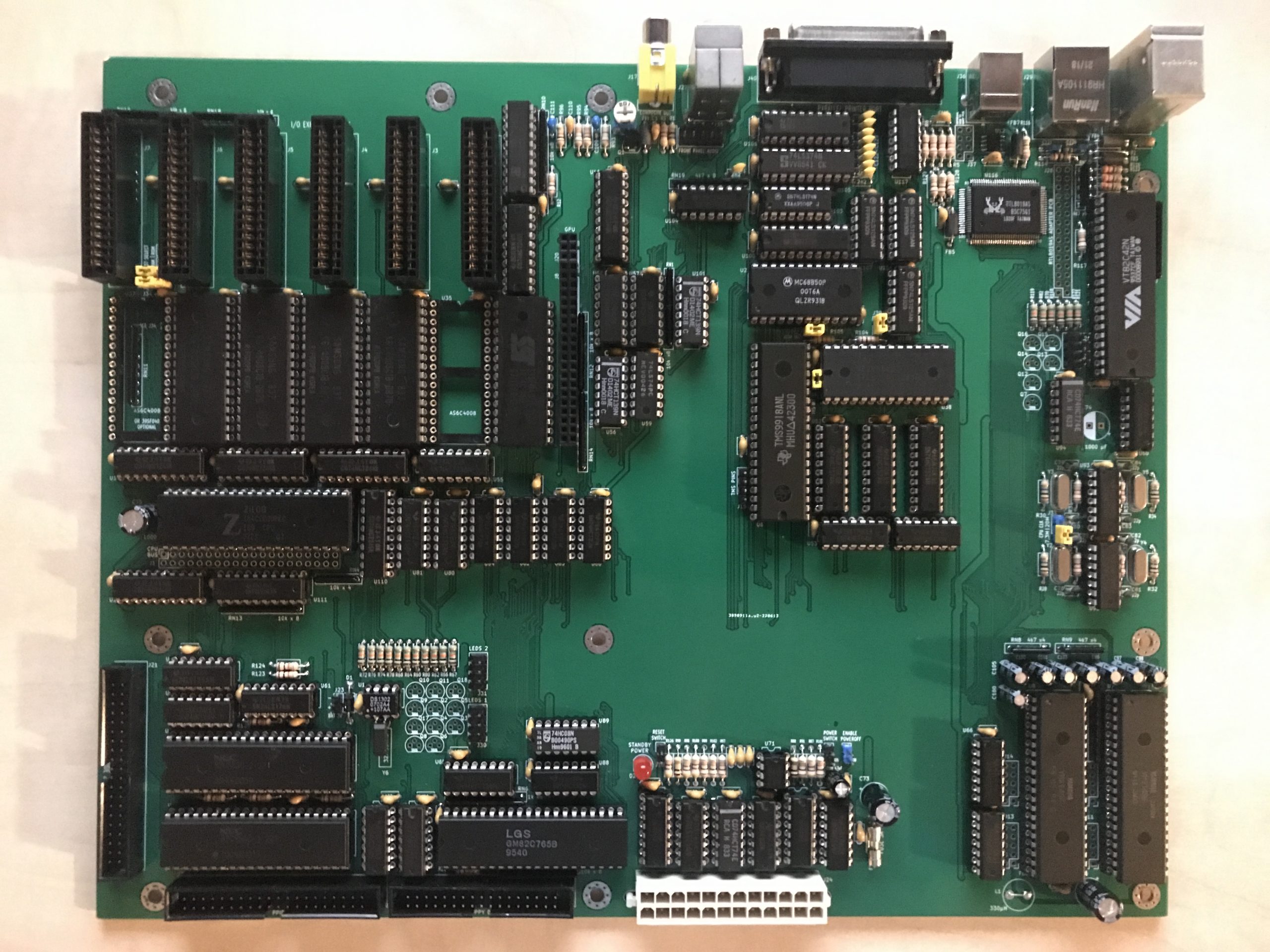
Here is a photo of the assembled PCB. At the top left are the expansion slots, and there is a double pin row connector for the future GPU expansion I am planning to make.
There is a little unused space on the PCB, I planned the design to fit the PCB space, but then found there is some free space left over. This is because of needing to move the lower case holes down to the ATX case standard positions to be able to fit all the design areas. I don't think I will design another revision, so for now I just leave the design as it is.
