
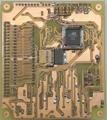
The Micro-ZX81 is a ZX81 project in SMD with a double sided PCB. It’s dimensions are about 10 x 8.7 cm.
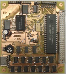
The main reason for me to design this project is to create a very small ZX81 on one single PCB. This PCB will even fit inside an original ZX81 case… Or something else even smaller of your own choice?
Another reason to do it is because I wanted to create a ZX81 which uses better logic than the ZX80 to ZX81 solution, while still trying to maintain as much compatibility with the original ZX81 as possible. You might say, a kind of purist approach to the ZX81. Most of the technology is taken from Wilf Rigter’s very excellent ZX97 Lite design. Wilf replaced many of the ‘bad design’ RC timing circuits of the ZX80 and ZX81 modifications and replaced them with his own ‘absolute’ digital versions, with which I mean, he didn’t use any timing compensation with capacitors as Sinclair did with the ZX80 and as used in the ZX81 slow mode modification. I believe at the time with the ZX80, sinclair did this to save needing additional ICs and reducing further costs. Of course, in our case, we would not need to save any ICs persé because they cost ‘hardly nothing’ and have quite a small footprint. I prefer using ‘neat’ circuits to using strange logic to reduce component numbers, and I don’t like to use diodes and transistors instead of logic ICs. But that is just my personal preference. Finally, the ZX97 generates a super solid tv picture, that was another consideration. As expected, I am happy to report, my prototype Micro ZX81 has the same great picture as the ZX97 Lite does, I am quite happy with it.
In short, as said, I based the designs on the ZX97 Lite, but left out the memory decoder and some other small circuits which are not a part of the original ZX81, instead I used Kevin Baker’s Memory decoder for using a standard ZX81 8K ROM at the bottom addresses, and mapping the rest as RAM. The RAM chip I used is a bit large perhaps but necessary as I wanted the full 56kb of available RAM. 62256 was too small. I happened to have some 681000C type smd chips available so that was the choice. As for the EPROM, actually we would only need a 2764, however since we cannot easily buy those in PLCC package, I decided to choose for the more easily available OTP 27256. I hope it was a wise choice, since we don’t know what manufacturers will do in, say, 10 years… In future designs, perhaps when I combine several devices with this ZX81 design, I could use the same 27256, and this time include the specific software for the expansions in it’s free areas and include the memory decoder circuits of the devices to address to the correct area of the 27256. Some examples: Floppy drive/IDE DOS software.
I would say the difficulty level is about average, it is a very doable project as long as you are patient, careful and precise. It is all relative of course to predict another person’s skill. If you plan to build this excellent project, I would suggest first reading this whole article where I have put a lot of useful information. In general, it is a good idea to first look at the board where everything should go, and strategically plan to solder in all the components in such a way that you are not hindered by other parts while soldering the smd components. A few examples: soldering the Z80 IC’s socket should be done later rather than sooner because the top resistor network is a bit near to it. The diodes for the keyboard matrix should be soldered before the keyboard connector next to them because they are quite near to eachother.
I recommend for starters to use a magnifying desk light with TL light source, or at least TL lighting and a magnifying glass on a stand. This will make your work much easier, and it allows you to carefully examine your soldering work.(which I recommend)
Some useful advice: When developing the PCB, it is best to use some additional PCB material around the board to keep it in place. You can paste the additional material around the PCB on the transparent film. First it’s best to allign the sheets of film together without the board, then place the board to be developed between the additional strips of PCB which you pasted to the bottom film. This way, when you want to turn the board over for developing the other side, it won’t shift relative to the layout film. At least, this is how I did it. Don’t be too worried, a slight shift between the top and bottom layer is acceptable. You can check by drilling some of the small via holes. Solder can sometimes cover up minor imperfections.
Just before you plan to solder, have a careful study of the PCB with a TL light source underneath and above it, use a magnifying glass to follow all the tracks and make sure there are no broken tracks or short circuits between tracks.
Via’s: there are many via (top-bottom) connections on the board. These should be drilled with 0.5 mm drill, or smaller if you could find one :). Next you can use a small core wire from for example a 220V mains cable which has multiple smaller wires inside and about 1,5mm2 diameter.(where usually the core wires are a bit stronger than other type of wire) You can strip the cable and use it’s thin wires. The reason I recommend it is to get a reasonably strong, yet flexible thin wire. Too thin and it might break during the work, but too thick and you would end up with very thick solder points which will give problems when soldering the ICs on top of them. What I did is to use long thin wires, and to ‘weave’ them through all the via holes just as if you are sewing something. Here you should always cleverly regard the direction you are weaving to, so that it is suitable to easily solder the wires without making accidental short-circuit soldering. Also, observe to keep the wires neat and tight to the PCB, as in this way the solder points later will be as flat as possible, which is what you will want. After all the wires are ‘woven’, they can carefully be soldered with a needle-tip soldering iron(which should be used for this entire project on all soldering work). As said, observe here to keep the little solder points as flat as possible. Try to use thin solder, for example 0.35mm solder. After soldering it is a matter of cutting all the wires with a miniature wire cutter(preferable side-cutting model with it’s jaws as small and pointy as possible. After the via’s, you can solder in the ICs and resistor networks. Here, try to keep them as level as possible(since there will be via solder points underneath). It helps to first solder two opposite corner pins. Then you can still position the IC to get ideal placement. A tip for soldering: After the IC is attached using the first two pins, try to slightly bend the remaining pins toward the PCB pads if the distance is bigger. That way, the soldering is much easier to do as you will find.
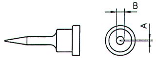
An example of a needle soldering tip
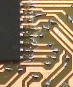
A close-up of some via’s
SMD components (capacitors/resistors/transistors/diodes etc):
It’s best to place them with a small tweezers until reasonably in the right place. Then you can solder one side first, then use the tweezers and heat the same solder point so you can ideally adjust the location until it is perfect. Then when the solder is solid, you can solder the other side and the component is perfectly straight. For 0805 componants, try not to heat the second solder point too long as it will distribute the heat to the other side and the component becomes loose again. A final advice for such parts, since we don’t have soldering masks, be careful to place them ideally straight so you can prevent short circuits.
About the EPROM, it is a PLCC version of the 27C256, I used an OTP type. It is possible to solder in a PLCC socket as well. For this, I would advise to take out the bottom plate of the connector so you will be able to reach the smd legs of the connector. Later remember to put in some tiny paper sheets to cover the PCB’s tracks and via’s underneath or the EPROM might accidentally touch them. What I did is to cut a strip of paper, fold it to about 4 layers and deposit it at the bottom of the PLCC connector. Then I placed the EPROM. Soldering the socket’s legs is a delicate task so take your time for this.
For the connectors, I used the same technique as implemented in the other projects, simply used precision IC sockets and cut them to size to make the PCB connectors. It is just as easy to make a mating connector with the same sockets, except this time you can solder the wires into the IC openings. The pins at the bottom become the connectors. A few tips while soldering the connectors: use another connector strip inserted into the one you are soldering. As during the solder work they tend to heat up, it can prevent melting the pins out of shape. The connectors should be soldered last.
For PAL TV system, place jumper J9. Two jumpers must be placed for border and background colour selection. My advice is to place them as in the example pictures, then during first testing, adjust P1 from low to high until you see that the black area of the K cursor is completely black
Important:
please note that since this is a double-layered project, some of the top to bottom connections are not done by via’s but by the component pins. This applies to some connector pins, but also for example to the Z80 Processor itself, the crystal, etc. Always watch this carefully because in the cases when the top layer connects a track or power plane to that pin, it must be soldered at the top side as well. Use a needle-tip soldering iron and thin (0.35mm) soldering wire. Allow the solder enough time to flow in place between the pin and the pad. It looks more difficult than it is, it is simply a matter of using a small soldering tip and thin soldering wire, and to find the most convenient angle of the soldering iron. You can start to practise this with some easier pins first.
Ideally, we would like to have manufactured PCBs with a soldering mask for this kind of project. I have been looking at some companies that offer to download some design software, you can draw a PCB layout and then directly from this company order a PCB. I noticed that the prices are relatively much more reasonable, especially compared to before this kind of option was available to us. However, using such a company requires yet even more work for me since I need to familiarize myself with the software, and redo the whole design from scratch. That is why, for now, I have decided not to do this work yet. In the future, I might be tempted to have a try however.
Another note:
Any job becomes much easier to do when you have the right tools for it. I can’t stress enough the importance of this. Try to use tools that are suitable for this kind of small scale work.
Please before building have a look at the photos page of this project where I have purposely included some higher resolution photos of my prototype work in order to illustrate how I have built the board. Do note the capacitor C12 in the middle of the board which I have soldered diagonally when I noticed the footprint in the PCB layout was not wide enough. Sometimes a little improvisation is needed.
As usual, the PCB layout files are not included in the web pages to save web space. Simply email me at with a request, and don’t forget to mention which project you would like to build.
IMPORTANT: Small modification needed:
Please note that I have not included 5 pull-up resistors at the keyboard input port J8. Have a closer look at the pictures of the bottom layer in the Micro ZX81 pictures section to see how I did it. You also could take a resistor network of 47K x 5 and solder it to the pins and use a wire for the VCC connection. If you only can buy a 8x or 9x resistor network, you could use a strong but sharp pair of cutters and cut off the remaining 3 or 4 resistors, you can simply cut through the resistor network.(do make sure to measure the 5 resistors) Without this modification, the Micro ZX81 works fine, except the keyboard won’t work.
RoHs:
Regarding choice of soldering wire: yes, at this time we do have something called RoHs which restricts the usage of dangerous materials and chemicals in products, therefore we now have available soldering wire which does not use any lead in it’s alloy. However, be advised that such soldering wire has a higher melting temperature than lead-alloy soldering wire. You might find that lead solder is much easier to use than such RoHs compliant solder because lead-alloy solder is much more fluid. Yes, lead is not healthy for humans, but it is my opinion that when we solder something small at home, it is not that bad to use lead solder as it would be for example during industrial production, where of course the amounts are much larger. You could use a small ventilator to blow away the vapour while soldering. That way you can reduce exposure even more. This is good practice of course also for RoHs compliant solder. Everyone must choose this for themselves which type they will use. I merely want to point out a difference between the two.
Debugging the project:
I recommend to carefully examine the soldering work when finished, use a magnifying glass and if available a powerful light source both underneath the PCB and above it. (the source below can shine through the PCB material and enables you to study any possible short circuits) Study each IC pin and make sure it is properly connected to the PCB. If you cannot find the problem still, print a copy of the schematic and measure each connection one by one. When a connection is confirmed, you can use a coloured marker pen to mark that connection in the schematic. I would suggest using a logic probe to check if the CPU is alive, for example checking it’s clock pulse, IORQ and MREQ to see some activity. Also probe it’s address lines for activity, and finally check the signals NOP and ^KBD for activity
General ZX information:
Display Screen Type
The Micro-ZX81 produces a black and white screen on a television set. I have included two jumpers in the design with which it’s possible to select the border and background color. (also see jumper descriptions) The Micro-ZX81 has a Composite Video output which means you will need a seperate A/V input (Cinch, SCART, DIN, BNC etc.) on your TV to connect the video output of the Micro-ZX81.
Normally the Micro-ZX81 operates in character mode which means that only characters in the CHR$ set are displayed on the screen, however, since the ZX81 has been introduced, several High-res software solutions were invented that allow a high resolution display on the ZX81 of which every pixel is seperately programmable.
Tape Storage of your Programs
If you plan to use an audio device such as a cassette recorder or your PC soundcard for saving and loading, you can make use of the Micro ZX81’s Tape input and output ports. The ‘EAR’ port(J12) is the ZX81’s audio input port, connected to the Earphone output of the cassette tape recorder, and the ‘MIC’ port(J11) is the ZX81’s audio output port, connected to the Microphone input of the cassette tape recorder(or PC).
I did use a different value in the circuit diagrams for some parts because with the R/C values as in the original Sinclair schematics I had problems recording programs through the MIC output. After some experimenting I got good results with the values as in the current circuit diagram.
Also there may be problems with the keyboard being slightly unreliable especially with long keyboard wires (capacitive), and also with loading programs from tape or PC soundcard. These problems could be solved by using a 74LS245 instead of a HC type for U23, which is the input port for both keyboard and tape input. An LS type will be much less sensitive.
Keyboard
For those not familiar with the ZX81 hardware, the keyboard that is used with the ZX81 is called a matrix keyboard. This means that all the keys used are mapped in a matrix position. When a ‘row’ line is connected to a ‘column’ line by a keyboard switch, it will be registered by the computer and the action that goes with this keypress will be executed by the computer. The ‘row’ signals are located in J10 and the ‘column’ signals in J8.
The row signals of J10 are then devided in two groups of 4 signals that pair up with the 5 column signals of J8 to make a block of 4×5 keys. Two of these blocks then add up to 40 keys total. The matrix keyboard is more clearly illustrated by the following table:
Block1  J6-1: J6-2: J6-3: J6-4: J6-5: Block2  J6-5: J6-4: J6-3: J6-2: J6-1:
J7-4:     1     2     3     4     5     J7-5:   6     7     8     9     0
J7-3:     Q     W     E     R     T     J7-6:   Y     U     I     O     P
J7-2:     A     S     D     F     G     J7-7:   H     J     K     L   Newline
J7-1:   Shift   Z     X     C     V     J7-8:   B     N     M     .   Space
Please note: most keys have several functions. These functions can be selected by the following methods:
1. Shift + Key
2. Shift + Enter: changes the cursor into a ‘F’ which is the ‘function mode’. In this mode, most keys have extra functions that are accessed by simply pressing the key after you have changed the cursor to ‘F’. After pressing a key, the ‘F’ cursor becomes a ‘K’ or ‘L’ cursor again.
3. Shift + 9: changes the cursor into a ‘G’ which is the ‘Graphics mode’. Keys pressed with a ‘G’ Cursor will result either in inverted text or in combination with shift some of them produce graphic symbols. The ‘G’ cursor will not change back by itself, you will have to press Shift + 9 again in order to change back to normal typing mode.
4. ‘K’ cursor mode. This mode results in a Keyword when certain keys are pressed.
5. ‘L’ cursor mode. This mode results in Letters when you press the letter keys. You can however still use Shift+Key and ‘F’ + Key in this mode which in some cases also produces keywords and functions.
Also note: the ZX81 handles the ‘K’ – ‘L’ cursor transitions automatically. For example, when you enter a keyword with the ‘K’ cursor, it changes to ‘L’ and you’re able to enter variables, mathematical symbols etc.
As mentioned, J9 selects the TV standard: place it when you want 50Hz (PAL, for example in Europe); leave it out to get 60Hz. (NTSC, for example in the US)
Memory decoder
The ZX81 memory decoder operates as follows for the main memory blocks:
Memory map:
Mem Area: 0000-1FFF 2000-3FFF 4000-5FFF 6000-7FFF 8000-9FFF A000-BFFF C000-DFFF E000-FFFF
Normal:      ROM       RAM       RAM       RAM       RAM       RAM       RAM       RAM
/M1 low:     ROM       RAM       RAM       RAM       RAM       RAM       RAM*      RAM*
* during /M1 low, and certain other signal conditions, DFILE is read from RAM, and any memory access to the C000h-FFFFh area is redirected by the memory decoder to the 4000h-7FFFh RAM memory area. This is necessary to achieve proper display generation and continued stability while the ZX81 is executing programs in the higher RAM areas.
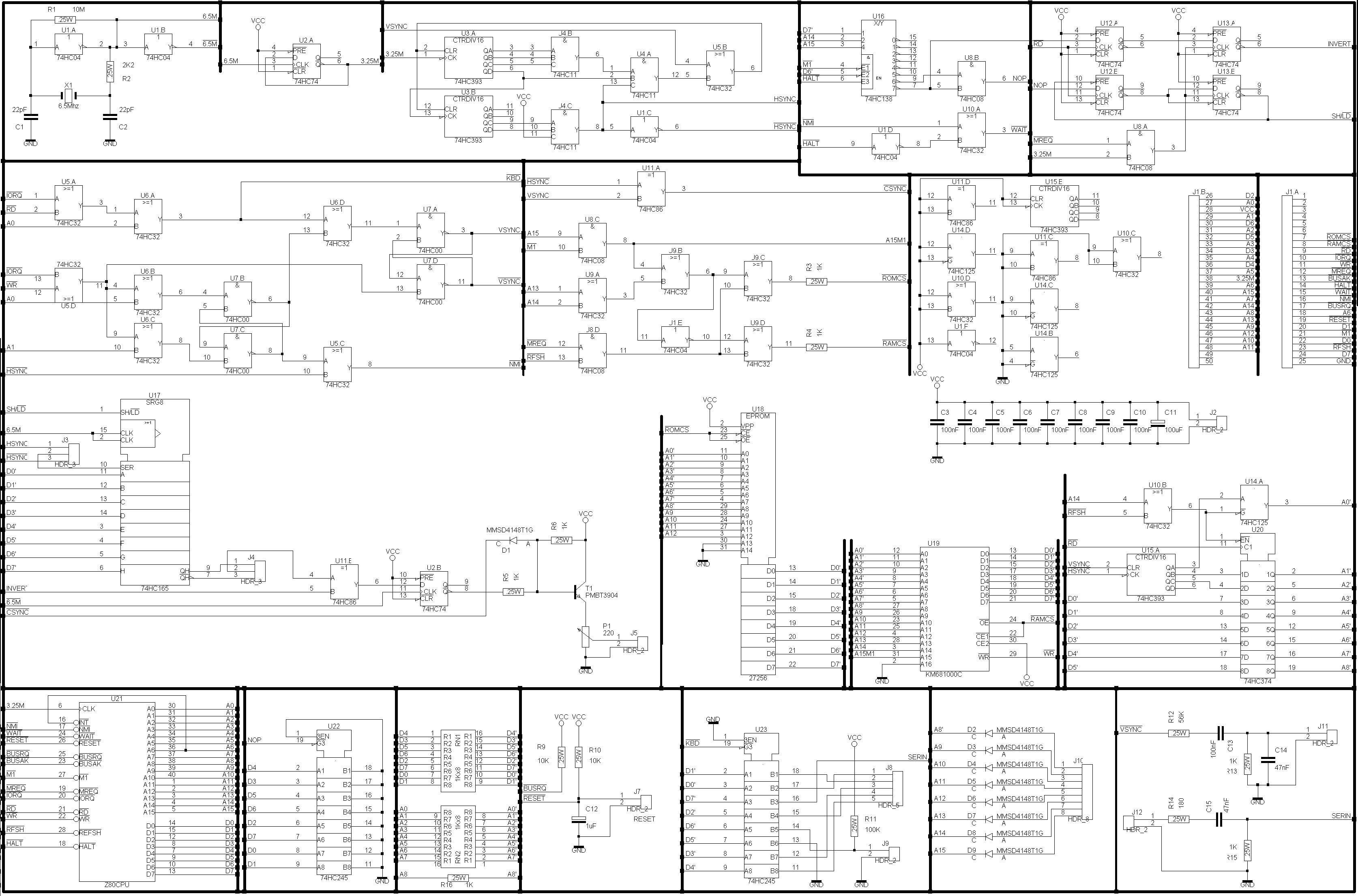
Micro-ZX81 Schematic
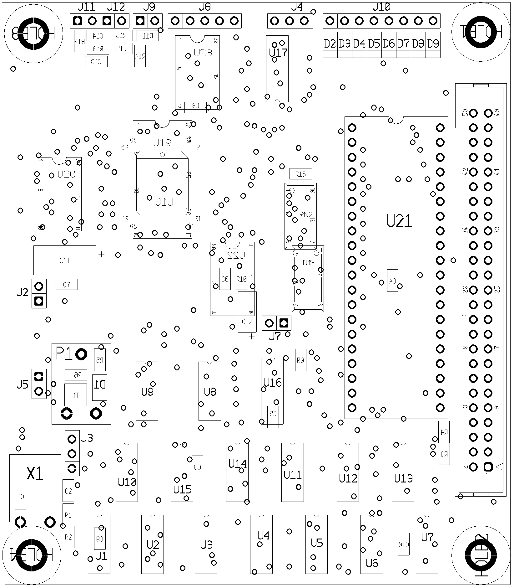
Micro-ZX81 Component Placement
Micro ZX81 Partslist
U1 – 74HC04
U2 – 74HC74
U3 – 74HC393
U4 – 74HC11
U5 – 74HC32
U6 – 74HC32
U7 – 74HC00
U8 – 74HC08
U9 – 74HC32
U10 – 74HC32
U11 – 74HC86
U12 – 74HC74
U13 – 74HC74
U14 – 74HC125
U15 – 74HC393
U16 – 74HC138
U17 – 74HC165
U18 – 27C256
U19 – KM681000C
U20 – 74HC374
U21 – Z80A CPU
U22, U23 – 74HC245
C1, C2 – 22pF 0805
C3-C9, C10, C13 – 100nF 0805
C11 – 100uF smd c
C12 – 1uF smd a
C14, C15 – 47nF 0805
R1 – 10M 0805
R2 – 2k2 0805
R3-R6, R13, R15, R16 – 1k 0805
R9, R10 – 10k 0805
R11 – 100k 0805
R12 – 56k 0805
R14 – 180 ohms 0805
RN1 – 8x1k smd sep. res.
RN2 – 8x1k smd sep. res.
P1 – potmeter 220ohms linear
T1 – PMBT3904
X1 – Xtal 6.5536 Mhz
J2, J5, J7, J9, J11, J12 – 2 pin header 0.1″
J3, J4 – 3 pin header 0.1″
J8 – 5 pin header 0.1″
J10 – 8 pin header 0.1″
J – flatcable header 50p
D1-D9 – MMSD4148T1G
You can find some photos of the Micro-ZX81 prototype at this page.(opens in a new window)
The copyrights of Sinclair Technology are the property of international computer manufacturer Amstrad. It is not allowed to use any designs provided in this website and/or any Sinclair Technology found elsewhere on the internet for any commercial use. It is not allowed to sell computers built with or based on plans from this website with the intent to make any commercial profit or gain. The sole purpose of the designs in this website is to use the designs for your hobby or for non-commercial learning purposes.