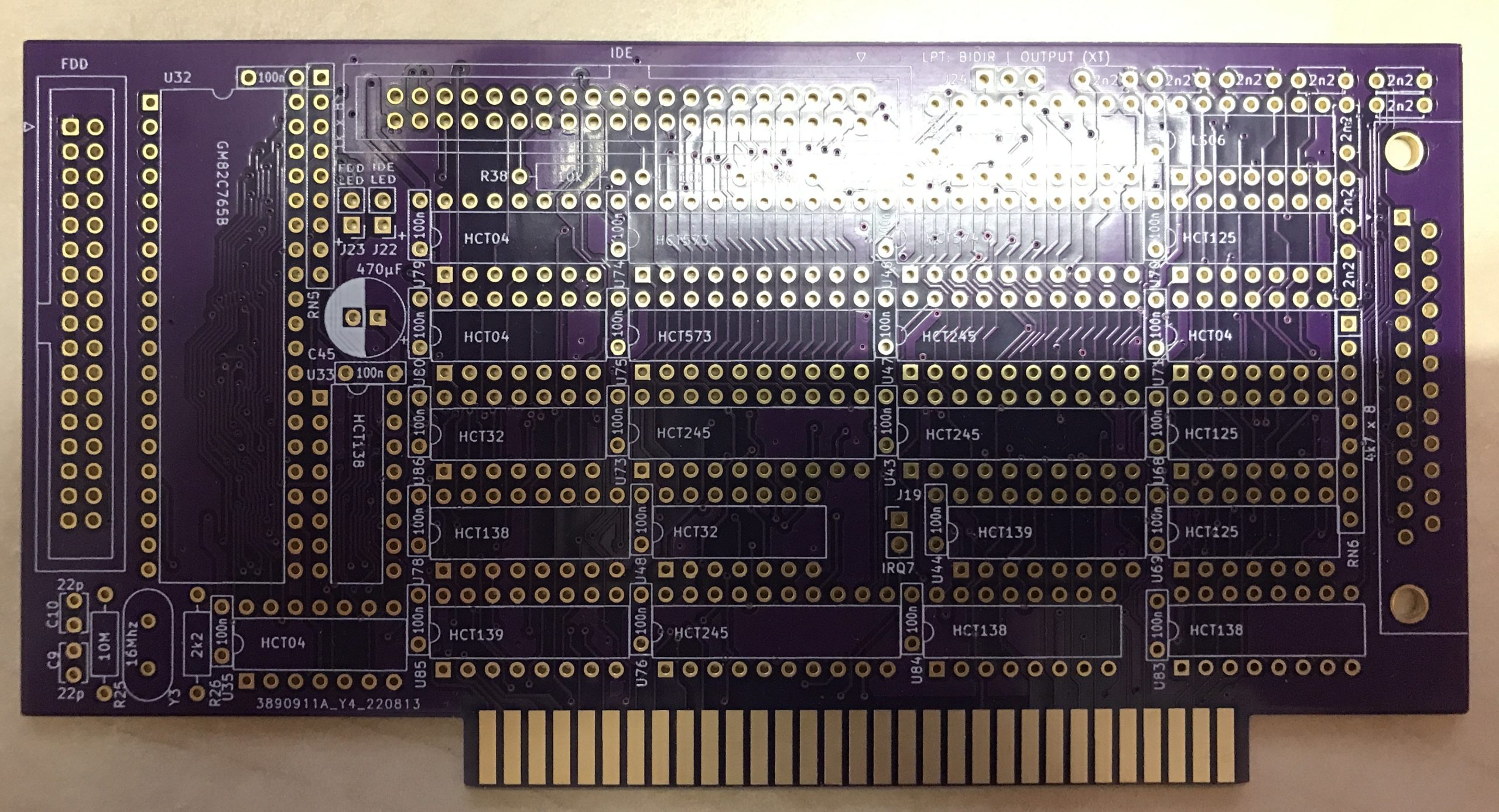
While developing my first revision Turbo XT mainboard design, I decided not to merely design another turbo XT clone of my own, I wanted the design to provide new features which could add value and functionality. I previously added an XT-IDE compatible variant card on prototype board inside an Amstrad PPC640 computer, after which I decided that my Turbo XT mainboard would also need to include an XT-IDE. Especially since it’s supported by a thoroughly developed BIOS from the XT-IDE Universal BIOS development Team. Furthermore, I studied the standard port addressing on a PC floppy controller and drafted an I/O decoder design to properly control the floppy drive controller chip according to the port schemes as found in various documentation. After spending much time to define the port numbers which I would need, I suddenly found a copy of this same information listed in the exact same way on an old scan on the internet. What a timing! Anyway, at least it served to indeed verify my determination to be correct. Finally I created my own variation of discrete parallel port design which is compatible with the standard IBM parallel port. I made a similar port on my Z80 mainboard on the second revision. I found that a small addition on this design from an unused output of one of the control registers would provide for bidirectional function as well so I added this function as well.
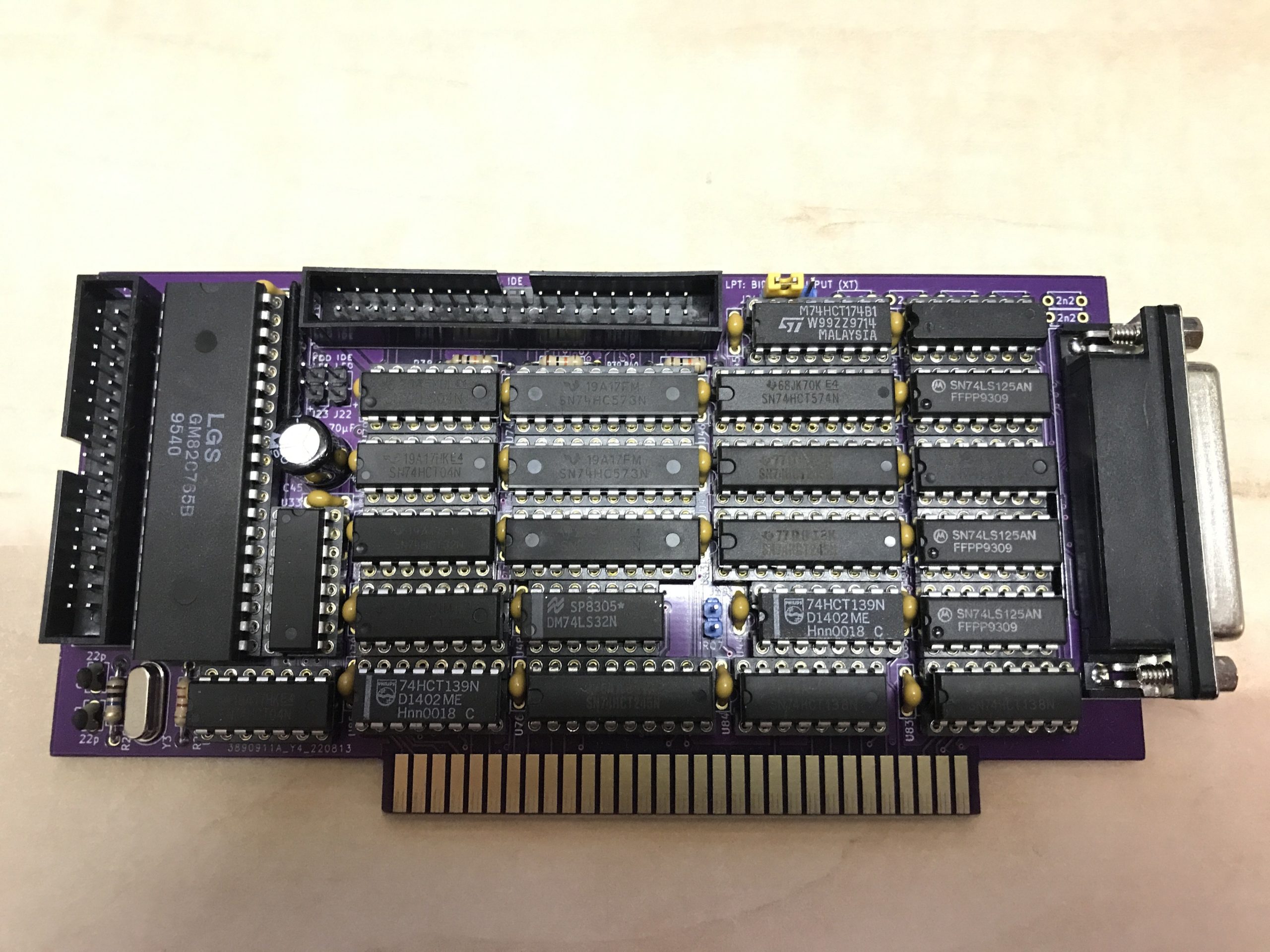
As I was ordering my first revision mainboard PCB which included all these circuits, in preparation of testing and debugging the whole mainboard, I decided to split out and design a card version of these I/O devices so I could test these interfaces separately and in advance on an XT mainboard. I included functionally identical I/O decoding on the card as in the mainboard design to be able to verify as much of the mainboard logic as possible using this separate adapter card design.
During my assembly and testing, the results were extremely positive! I remember previously being plagued by timing and stability problems on the Amstrad version hand wired prototype board, however after using the XT-IDE compatible logic on this PCB, once I got the right logic selection to support sufficient timing, from then on any harddisk I connected was properly supported by the XT-IDE universal BIOS. So all my previous problems were in fact due to the signal and power instability of my hand wired prototype. Another reason to realise I should be quitting the hand wired work forgood and opting to wait for PCBs to arrive from China in the future.
This adapter card is extremely useful to setup and install an XT PC with. The card can provide a harddisk, floppy drive for an initial boot, fdisk and format of the harddisk, and the means to connect to another PC using interlnk.exe to transfer the DOS files onto the harddisk after making it bootable and verifying proper booting. All these functions on a single PCB are in my opinion a good and useful combination.
Some technical facts:
XT-IDE compatible IDE:
Port 300 / 308
Floppy drive:
Port 3F2: Digital output register -> /LDOR = 0
Port 3F4: Main status register -> /CS = 0
Port 3F5: Data register -> /CS = 0 (A0 = 1)
Port 3F7: Digital input register -> /LDCR = 0
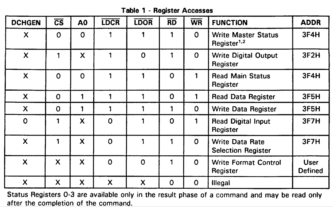
Here is the crucial bit of information for designing the floppy drive controller I/O decoding logic, which I came across only after I completed my own determination of the same information as above by going through lots and lots of documents and pages and filtering out all the info to conclude the same info as above! It’s so funny to find tons of info about FDCs in the IBM PC everywhere but no exact specifics as above how the I/O should function to do the controlling of this very common and popular FDC controller chip, I only found this specific info in one PDF document by Standard Microsystems on the FDC37C65 on page 16! Even when seeing the above table, you have to know what to conclude from the table to understand how and why this table is so important. Kudos and cheers to the person who drafted this very useful and important information! I think it was at one time long ago faxed to someone who requested the info, since the document had some fax letterheads above the pages!
This matter is a perfect example of how hard the process of designing an XT PC has been. Every time I encountered various design issues and uncertainties, and I had to dive into another logic and control area of the whole system. This process for me was composed of a long list of notes, checks, thinking over all the logic if it could be functional as intended, etc. for each design area and issue I dealt with in the whole system. Definately, on this XT design I have done the most verification and research, evaluation of logic, redo the design, draft tables, etc. of any project I have ever done! And after designing the circuits, I still reviewed them again, looked at things from all angles, rethink them, and decided to do them differently later! You can imagine my relief after ordering the PCB, which has a finality to it to let go of this process and call it complete!
Discrete LPT Port:
Port 378 -> LPT Port A Printer data bits, I/O
Port 379 -> LPT Port B Status bits, input only
Port 37A -> LPT Port C Various controls and IRQ if enabled, I/O
Thankfully the printerport was relatively straight forward, I changed some of the ICs to use different types of gates because I prefer to use those instead and think it’s a better method. Even though it needs a few ICs, I always prefer to use off the shelf logic ICs when possible.