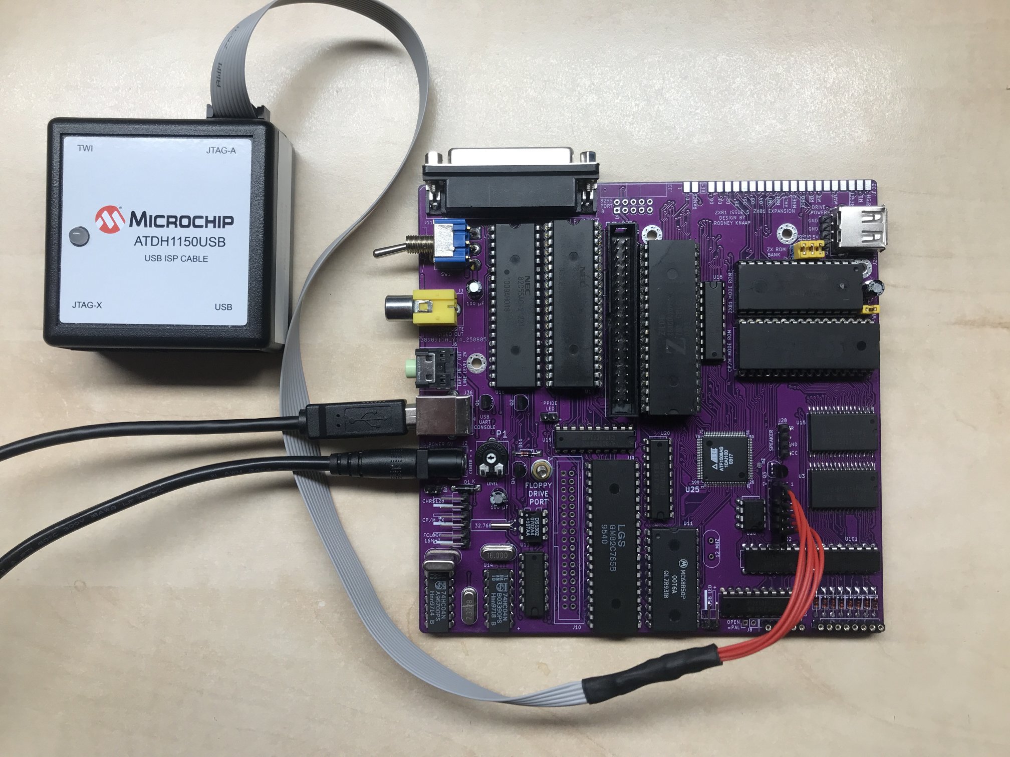
A ZX81 project based on CPLD technology, includes equivalent logic of ZX81 ULA functions based on ZX97Lite and combines ZX81 operation with ROMWBW compatible HBIOS and CP/M mode.
Ever since I started working on recreations of the ZX81 computer in the late 1990s years I always have seen the potential for more elaborate use of the ZX81 video display system in more advanced designs. During the early designs I envisioned a ZX81 or rather a Z80 based computer with more expanded capabilities, allowing the ZX81 to have access to a harddisk, floppy drive, an operating system, professional printer port, serial port, and possibly even USB devices.
Developing a new operating system is just beyond the scope of possibility since this would be a huge task to program everything from scratch and adding all the device drivers for the entire system. So I have looked at existing operating systems and software for the Z80. And there immediately the idea comes to mind to use the CP/M operating system since this potentially can support a wide range of software and hardware. From the Z80 PC project we can see the usage of ROMWBW, HBIOS and CP/M based on bank switching and memory management in HBIOS to expand the ROM/RAM capacity of the Z80 in order to support paged memory of much larger size, which enables running larger applications that can use much more RAM than the standard Z80 addressable 64KB. In fact, even similar memory capacity to the first PC/XT systems. So the idea is to design a ZX81 based computer which is capable of controlling a range of devices and larger memory capacity.
Resulting from my earlier CPLD based work I have gained a lot of experience designing integrated hardware systems where a lot of logic circuits are migrated into programmable logic. The CPLD is a primitive and more limited version of an FPGA chip which came out before FPGA technology evolved further. The advantage is being able to support 5V logic design while at the same time using the capacity for system integration as well.
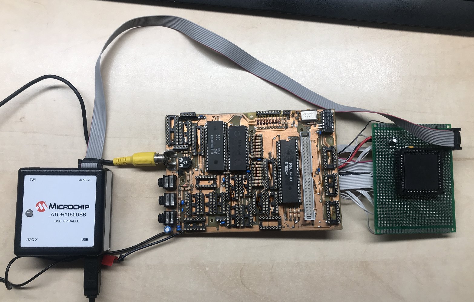
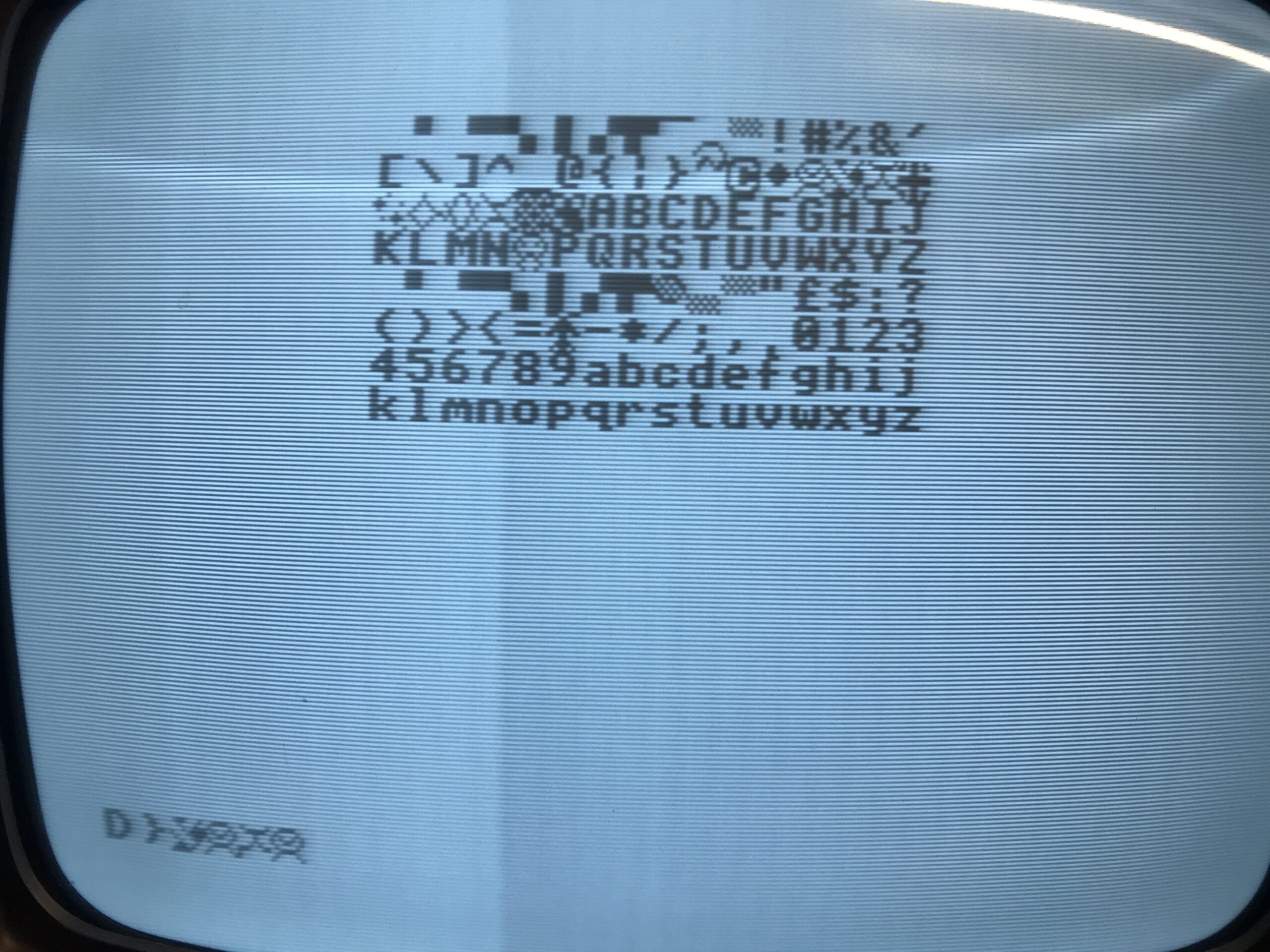
So I proceeded to create some CPLD test designs to get a ZX97 based computer up and running where the bulk of the logic is migrated into CPLD logic programming. I modified my existing ZX81 Issue 4 prototype by wiring it to a board containing a 84 pin PLCC package CPLD chip. One of the challenges was designing new logic which was capable of performing the same functionality as the ZX81 ULA chip which allowed the ZX81 to have a smaller component count and supported a much cheaper fabrication of ZX81 computers.
The ZX81 video display system
as explained by Wilf Rigter
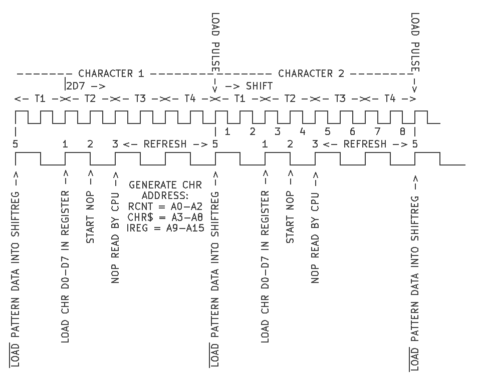
According to Wilfs explanation we have these timing instances as indicated in the diagram above:
- Each character code (CHR$) byte in DFILE is addressed by the CPU PC, on the rising edge T2 data is loaded from DFILE into the 74HC574 : bits 0-5 and 7 into 7 bits.
- On the falling edge of T2, the NOP circuit forces all CPU data lines to zero.
- On the rising edge of T3 the low data lines are interpreted by the CPU as a NOP instruction.
- During T3/4, the CPU executes the Refresh cycle and ROM address lines are generated with I register on A9-A15, the CHR$ latch on A3-A8, and the ROW counter on address lines A0-A2.
- On the rising edge of T1, pattern data from the EPROM is loaded into video shift register and 8 video pixels are shifted out at 6.5MHz
- If bit 7 of the CHR$ latch equals 1, then the serial video data is inverted.
- The CPU increments the program counter and fetches the next character code.
- This repeats until a HALT is fetched.
- HALT opcode bit 6 = 1 and is therefore executed (no NOP).
- The SYNC timebase generates a HSYNC pulse independend of the CPU timing and the ROW counter is incremented.
- The halted CPU continues to execute NOPs, incrementing register R and samples the INT input on the rising edge of each T4.
- When A6, which is hardwired to INT, goes low during refresh time, (bit 6 of the R reg = 0), the Z80 executes the INT routine (below 32K).
- CPU returns from INT and resumes "excution" of DFILE CHR$ codes.
- The process repeats 192 times and then INT routine returns to the main video routine, turns on the NMI latch and switches back to the application code.
How to proceed from here
After I achieved this hand wired equivalent design based on a circuit foundation of the ZX97 (which is very similar to the ZX80 and ZX81) I decided to move on to the next phase of the design concept, which was integrating the ZX81 CPLD based design with a ROMWBW capable system containing the ROM/RAM memory bank switching system and several IO interfaces which are all supported by ROMWBW, HBIOS and the CP/M operating system.
I did so in a way where we have the ZX81 hardware / software and CP/M hardware / software merged into a single hybrid computer system with a programmable CPLD system controller which is in charge of all the system operations. The programmable CPLD logic core allows completely flexible development of the resulting computer system design, and in addition supports different modes of hardware and software operations to coexist in the same computer. The idea is to use CP/M as the operating system to load software into the computer, allowing to dynamically expand the ZX81 operations.
By being able to boot CP/M on the ZX81 and then use CP/M for supporting ZX81 functions, we could potentially elevate the ZX81 computer into a system similar to a PC. To what degree we are able to do this will depend on software development to support the ZX81 core computer. Using CP/M we can overcome the severe limitations of the ZX81 computer which is dependent on certain ROM code and I/O mechanisms which is much less flexible for expansion by loading CP/M which could then be able to initiate ZX81 computer operation in a wide range of configurations. The CP/M operating system is able to run outside of ZX81 core RAM and ROM space, where it is able to do file I/O operations to the ZX81 RAM space, which is reconfigurable as well for example into covering the entire ZX81 memory space in RAM, where we even have 128KB of RAM available through additional banking mechanisms. Reconfiguring the computer for different operating modes can be done by simple IO operations setting various register bits which result in switching all the hardware into different modes.
For setting an initial base level functionality I have designed a single net in the CPLD which switches ZX81 or CP/M mode. As a starting point to make it possible to develop from, CP/M mode now supports all the ROMWBW/HBIOS supported devices present in the design.
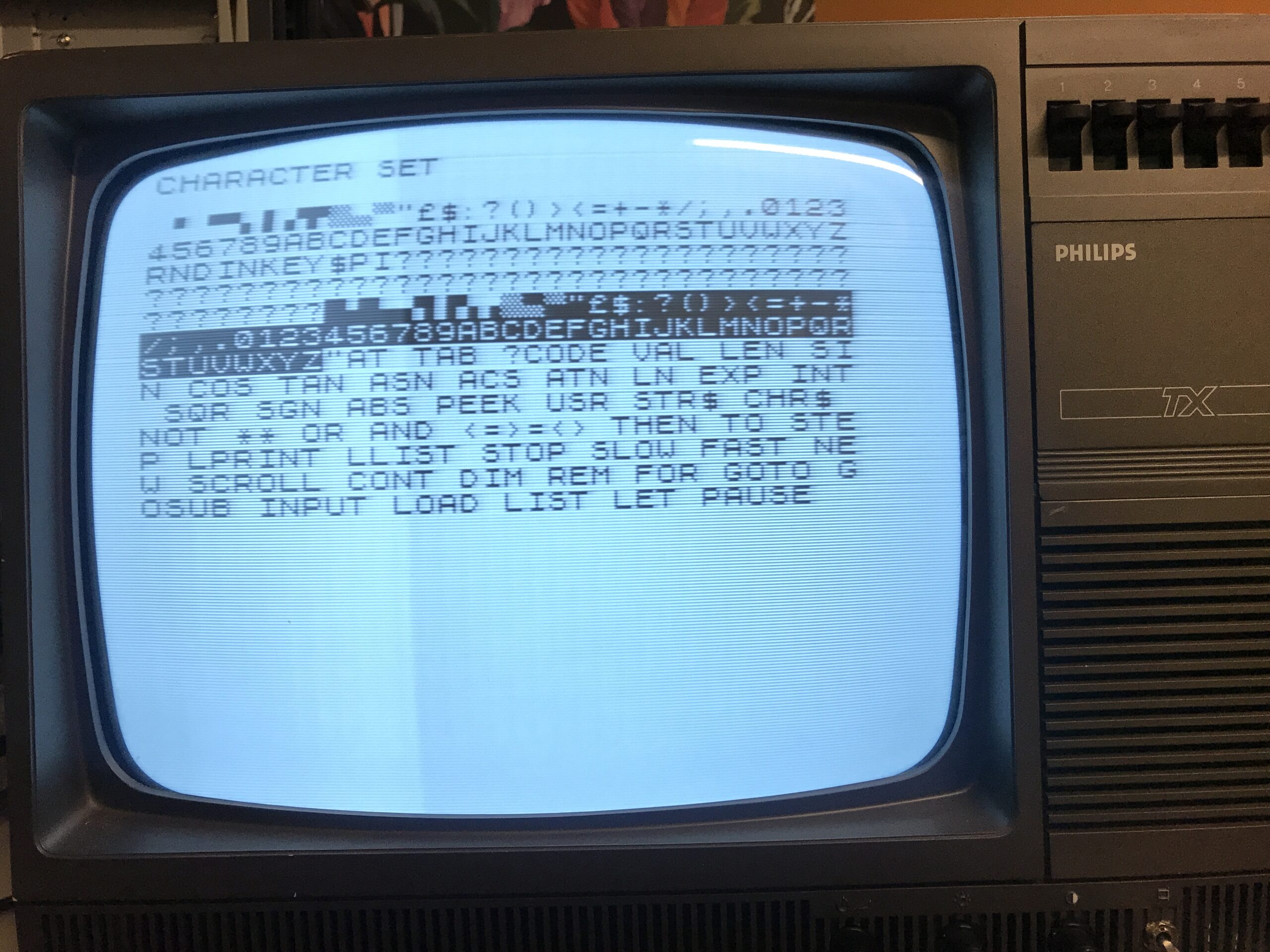
The next phase of development needs some talented ZX81 / Z80 programmers to join with this project to develop more elaborate modes of operation. One idea which would elevate the CP/M mode to completely new levels would be to design display and keyboard (console) drivers for CP/M and HBIOS. This would enable the operating mode of the computer to be able to boot to CP/M and use the ZX81 keyboard and video display system to show the CP/M console.
Once that is established, the next phase would be to write software for CP/M for loading programs and ROM code into the ZX81 RAM and switch to ZX81 mode to start the ZX81 native program. And a mechanism could be created to interrupt the ZX81 and switch back and forth to CP/M operation for example for saving programs and data to any CP/M disk and any variety of operations for the computer.
Having CP/M running on the ZX81 display system also enables a wide range of CP/M based software to run on the ZX81 computer hardware as well, thus expanding the ZX81 into a full blown CP/M system.
The ideas are basically limitless now the ROMWBW, HBIOS and CP/M base is available on the computer which potentially can make the ZX81 computer much more powerful and capable. Further ROMWBW expansions could also be connected to the ZX81 expansion port. The CPLD has various outputs connected to the expansion port which can potentially make the expansion capability much more elaborate and allows the expansions to be supported in CP/M as well.
Feature list
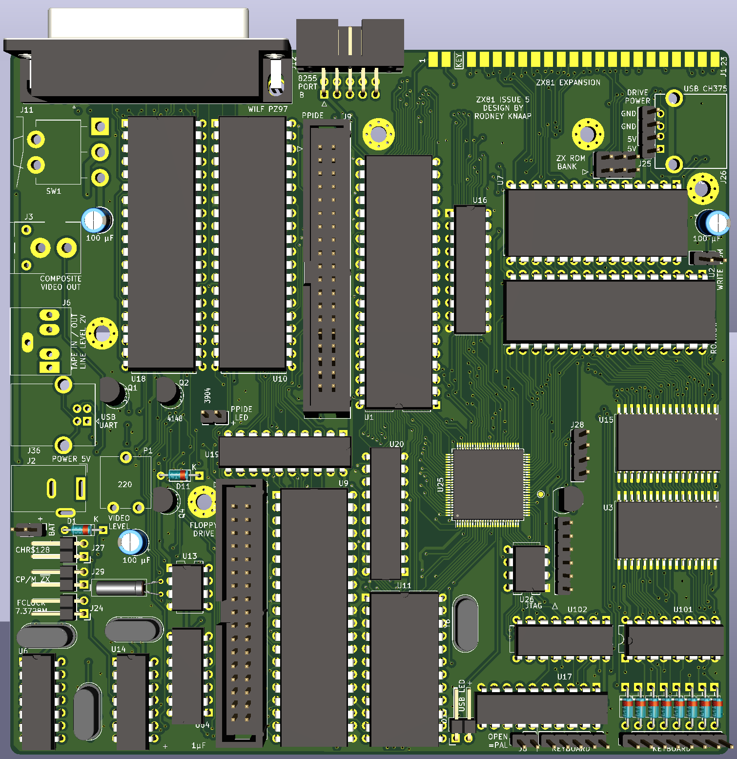
- internal power switch
- 512KB ROM for ROMWBW HBIOS and CP/M
- 1,5MB of dedicated SRAM for running CP/M
- ZX81 ROM is 64KB W27C512 chip, which amounts to 8x the ZX81 ROM size, 3 jumper positions available on the PCB for selection of the ROM page
- 128KB SRAM chip supporting ZX81 display, MA14, MA15 and MA16 on the ZX RAM are possible to be generated with the CPLD to support memory paging operation, swapping 16KB pages of RAM
- all of the memory chip enables are output by the CPLD so these are reconfigurable
- HD floppy drive controller (freely configurable port addresses of the FDC chip in ZX81 mode and CP/M mode)
- PPIDE interface
- ACIA serial commmunications
- USB to Serial CP/M console input for PC connects with the ACIA
- serial RTC chip Dallas
- Wilf Rigters PZ97 port using a 8255 and parallel port connector
- PZ97 8255 Port B connects to separate header including power pins at back of case for custom I/O development
- power output header inside case for powering drives
- CH375 universal USB controller chip with a USB A socket at back right of the case
- tape I/O at line level, 2V amplitude ZX81 tape loading using a 2 stage transistor circuit, fully verified
- FCLOCK input on the global clock input pin of the CPLD for providing a faster clock source for development purposes
- 7.3728MHz oscillator connected to CPLD input for CP/M mode standard clock frequency
- 16MHz oscillator for FDC could be supplied to FCLOCK with a jumper for clocking the CPU or other circuits at higher speeds
- NE555 based system timer onboard, generates low frequency timing pulses, for example at 880Hz vintage PC speaker beep frequency
- self RESET function present in the CPLD, RESET period will be defined by choosing NE555 timer RC component values
- clock pulse to the expansion connector is able to be generated completely independently from the CPU clock to support any type of expansion clock speed
- separation resistors on ZX81 ROM and RAM chip enable signals allow external disabling of ZX81 memory if needed
- speaker output pin present on CPLD using a transistor output stage, supports sound experimentation and development by connecting a speaker
Further information for building this computer
Please carefully read all the terms and conditions of usage and the license issued with any of my designs, and agree with all these conditions and the license, before building this computer. The separate conditions are listed below, and the license is bundled in the GitHub page of the project.
The computer designs are published on my GitHub page.
There is also a thread which I posted on the VCF forums.
On the GitHub page the PCB gerber files and quartus design files can be downloaded.
These are under development and will evolve if and when software and drivers are created for this computer.
So we will need the help of some talented ZX81 / Z80 programmers to have the full range of operation that the hardware is able to support. Please get in touch with me and we could work together for allowing software to control the computer by I/O and memory operations as needed. The hardware can be configured in any mode of operation necessary.
Also keep in mind that we could use high resolution display in CP/M mode to expand the numbers of displayable columns on the CRT output. For this purpose the console drivers need to be created for supporting ROMWBW and HBIOS which also allows CP/M to use the ZX81 display output. CP/M mode is not limited to anything that the ZX81 screen needs and can operate beyond that limitation on any level desired as long as the ZX81 display circuits and/or even any alternate display logic ideas able to run inside the CPLD to support any advanced display modes we can think of. I am very sure that talented ZX81 programmers will have many ideas what they would love to do on the system when software space and hardware are no longer bound to the ZX81 design but instead can operate in any type of circuit as long as it's possible in the existing reprogrammable hardware. CPLD logic will be able to support switching operating modes between the ZX81 and CP/M mode.
Purpose and permitted use, cautions for a potential builder of this design
This project was created for historical purposes out of love for historical computing designs and for the purpose of enabling computing enthousiasts with a sufficient level of building and troubleshooting expertise to be able to experience the technology by building and troubleshooting the hardware described in this project.
Besides the GPL3 license there are a few warnings and usage restrictions applicable: No guarantees of function or fitness for any particular or useful purpose is given, building and using this design is at the sole responsibility of the builder.
Do not attempt this project unless you have the necessary electronics assembly expertise and experience, and know how to observe all electronics safety guidelines which are applicable.
It is not permitted to use the computer built from this design without the assumption of the possibility of loss of data or malfunction of the connected device. To be used strictly for personal hobby and experimental purposes only. No applications are permitted where failure of the device could result in damage or injury of any kind.
If you plan to use this design or any part of it in new designs, the acknowledgement of the designer and the design sources and inspirations, historical and modern, of all subparts contained within this design should be included and respected in your publication, to accredit the hard work, time and effort dedicated by the people before you who contributed to make your project possible.
No guarantee for any proper operation or suitability for any possible use or purpose is given, using the resulting hardware from this design is purely educational and experimental and not intended for serious applications. Loss of data is likely and to be expected when connecting any storage device or storage media to the resulting system from this design, or when configuring or operating any storage device or media with the system of this design.
When connecting this system to a computer network which contains stored information on it, it is at the sole responsibility and risk of the person making the connection, no guarantee is given against data loss or data corruption, malfunctions or failure of the whole computer network and/or any information contained inside it on other devices and media which are connected to the same network.
When building this project, the builder assumes personal responsibility for troubleshooting it and using the necessary care and expertise to make it function properly as defined by the design. You can email me with questions, but I will reply only if I have time and if I find the question to be valid. Which will probably also lead to an update here. I want to primarily dedicate my time to new project development, I am not able to do any user support, so that's why I provide the elaborate info here which will be expanded if needed.
This project was inspired by:
- Sinclair computers in the 1980s
- Wilf Rigter who helped me with my PCB designs in the 1990s
- the German ZX-Team who inspired me a lot by sending me their Magazin and kind letters and messages. Particularly Peter Liebert Adelt and Kai Fischer with whom I have had very pleasant and memorable contact in the 1990s years.
- Gary Kildall who invented CP/M, the concept of splitting the BIOS from software operation and so much more
- Wayne Warthen who created and manages the ROMWBW CP/M project development which is part of the basis of this project
