
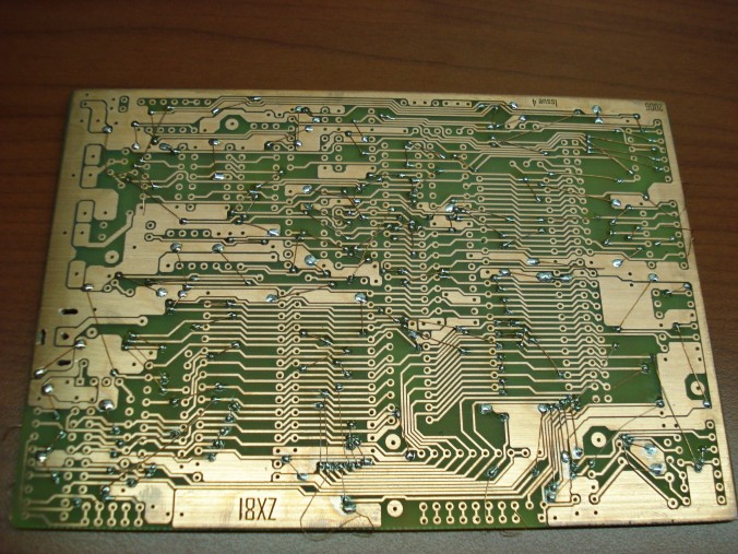
prototype of ZX81 Issue 4
Issue 4
The ZX81 Issue 4 is basically a Micro-ZX81 board which has DIP ICs and suitable dimensions and connector positions to make it possible to build the board into an original ZX81 case. Hence the name ZX81 Issue 4 since the original ZX81 boards by Sinclair were made until Issue 3. Feel free to have a look below at some more PCB photos and also check out the component placement page(button on the left) to see how tightly packed the ICs are on the board. I have assembled the schematic for the Micro-ZX81 from Wilf Rigter’s ZX97 Lite, Kevin Baker’s Memory decoder for 56kb and some other small bits. I took out some bits from the ZX97 Lite to get a final schematic that I feel is most compatible with the original ZX81 and has a chance to fit inside the ZX81 case. That was my goal in designing this project.
Repair your broken down ZX81 without needing a new ULA, and in the process have more memory too. The result will be a more stable and more durable ZX81 than the original. If anything ever breaks down, you can simply pull and replace the broken IC, unlike the original ULA. Less power consumption as well. Sounds like a good advertisement for ZX fans. This project is one of the most important reasons why I started designing and building ZX81 type of PCB projects, so that the ZX81 can be preserved and revived, or even recreated from scratch with a self built case and keyboard. The only requirements are some skill with PCB etching, some knowledge of electronics parts and some precision in your work. All these skills can be acquired even if not present. I will try to add some tutorials in the building tips section. Also in these project pages you can find valuable information and tips for building the projects.
How did I get the idea to do this now and why not before? First of all, during my first ZX design work I always focused on making single layer PCBs. At the time I felt that double sided PCBs are too difficult. Recently I started making double layered ones, and my relatively easy success with some initial SMD double sided PCBs (remember, I use home PCB manufacturing methods so through-hole metal plating is not one of my available technologies, which means, using thin wires and a soldering iron) gave me a taste for making more designs, this time with DIP ICs. I must admit, when I started to place the components on the relatively small board of only 10×14 cm in my CAD software(compared to two 10x16cm boards for the single sided Euro-ZX81 for example which means a reduction of more than 50% board space), I had some small doubts about whether this would even be possible using only DIP ICs. Then when I got more and more ICs as tightly packed as possible onto the board(again, see the component placement diagram), assembling most of the traces of those components as I went along, at last I realised that board space became so cramped that I almost didn’t have enough space to even place the remaining ICs onto the board! You can see this in the component placement section from the criss-cross placement of the bottom DIP ICs. The awkwardly situated holes for screwing the PCB to the upper shell and for passing through the case assembly screws of the original ZX81 didn’t help much either for saving space. The end of the story is, I got it done!! That time I worked until 2am to get 100% completion status, until close to the end thinking that perhaps it would become necessary to start again from scratch or use extra wires to make the final connections, but I did get it done after all… 🙂
A few side notes and pointers to remember:
– the expansion connector couldn’t be placed at the edge. Instead, I put it right next to the Z80. This saves considerable board space otherwise necessary for accommodating a lot of extra via’s and traces… The solution for expanding the ZX81 Issue 4 will be to use a small flatcable to take the connections to the opening in the back of the case. I imagine several solutions, one would be to leave the flatcable plugged into the ZX81 Issue 4 PCB. Another would be to make a male – female flatcable solution which ends up at the edge of the ZX81 case. Then nothing sticks out but you can still plug in a flatcable at the back of the case. This solution would be best when you find a method to attach the female connector to the case somehow. Also, the flatcable can be made more flexible by seperating the wires from eachother after the connectors are fastened to the flatcable making sure the order of wires is correct. If someone finds a nice solution for this, feel free to send in some pics so I can put them in the building tips section.
– the board needs to be, unlike the original ZX81, powered by a stabilized 5 DC power supply. Tip is plus 5V DC. I would suggest buying a 5V DC switching mode power supply, but if you can’t get that, you could make a small box with 9V DC in from the original ZX power supply (which looks great and nicely original!) and an output of 5VDC stabilized. This can be done for example with a 7805 IC with heatsink and some capacitors at both it’s input and output. At the input I would suggest 10uF, 100nf as closely possible to the pin 1 and ground pin 2 of the 7805, and a 1000uF and a 100nf closely placed as well at the output pin3. Having the power supply outside the ZX81 case only extends its life because there is almost no heat generated inside the ZX81 case which helps preserve the keyboard membrane.
– the distance holders of the upper shell of the ZX81 have some ‘X’ like plastic cross section shape around them to make them more strong, however I didn’t have enough space to accommodate the larger ‘X’ diameters. This means that part of the ‘X’ needs to be removed from around the plastic PCB supports to get a small ‘o’ shape close to the PCB. I would suggest using some cutting pliers like wire cutters with very small jaws. The remaining material around the plastic supports can be carefully removed with a hobby knife. Later when I actually build the board into a ZX81 case, I will make photos and post them in the building tips ZX81 section.
– the screws that go at the bottom of the PCB might need to be screwed using a filt or plastic ring between the screw head and PCB bottom to protect the traces underneath and prevent possible short circuits. Just have a look at the screw to see if it is better to use a ring.
– the keyboard connector positions are not compatible with the original ZX81 keyswitch strips. This is however not a problem because these strips need to be modified anyway to get a strong and reliable flatcable connection. If this modification is not yet described in the building tips section of this website, please have a look at the ZX Spectrum version which is at the time I am writing this already online. The modified keyboard connections can be any length you choose.
– it would be best if you still have the original ZX81 PCB because the connectors on this board are needed for this new PCB. You will need to solder off the three 3,5mm jack connectors(be careful not to heat the 3,5 mm connectors too long or they could melt, just try to desolder them a little bit at a time and blow at the connectors to cool them down in between) and both keyboard strip connectors. These keyboard connectors need to be used to modify the ZX81 membrane keyswitch strip connections.
– if you experience some problems with the keyboard, it might be beneficial to replace keyboard port IC U23 with an HCT or even an LS type 245 IC. I certainly advise to use precision DIP IC sockets for all ICs in this project so it will be easy to repair the board if ever broken down.
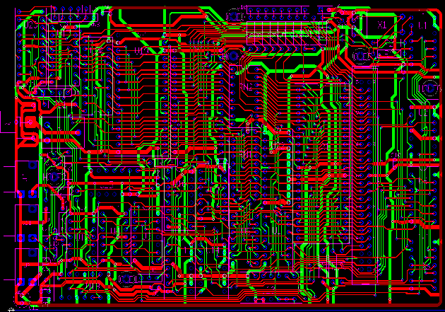
A screenshot of the board from my layout program gives a first impression of the layout
Some info about the PCB:
Total number of pins: 616
Total pins with connections: 571
Total number of via’s: 289
Total number of connections: 439
Number of ICs: 23
Project Description and tips:
PCB is now etched. Had some trouble with not dense enough, not straight enough, inconsistent laser printing on transparent foil, and some over developement by not covering the opposite side while developing. Finally got some reasonable result on a HP all-in-one laser printer. Next time I think I will get out my old canon LBP660 which I now remember I never had much trouble with… Anyway, I have a workable PCB etched now. I improved my PCB machine by buying a new air pump, as well as a new “air curtain” from an aquarium shop.(useful for getting such equipment) The pump has a double air output which I made good use of with my old and new air curtain tubes combined. Now there really was a strong air bubble flow through the etching machine which greatly shortened etching times. Always remember: the shorter etching times, the better. That’s what the professionals also do. Usually they tend to use machines which have a great etching liquid flow. Some techniques even involve spraying etching liquid onto the PCB. The more powerful etching, the thinner PCB traces can be achieved. I took out the one-way-valves from the air tubes which increased the airflow some more. Just have to remember to disconnect the air tubes from the pump after etching. I now keep the pump seperately which is much better than keeping it connected. Somehow the etching chemicals always found a way into the pump before which is from now on prevented. A next page I am planning is a how-to guide for your own home PCB setup with useful tips for getting the most out of your equipment. lately I am reading a lot about etching and PCB making techniques. Anyway, here are some pics of the not yet stripped and cut down to size PCB, so still 10x16cm in size:
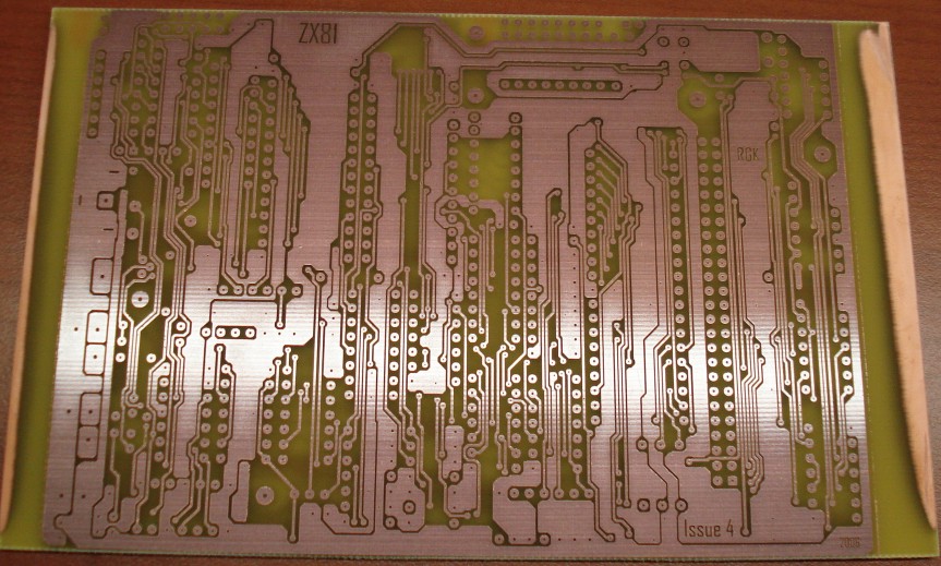
ZX81 Issue 4 top layer – just etched
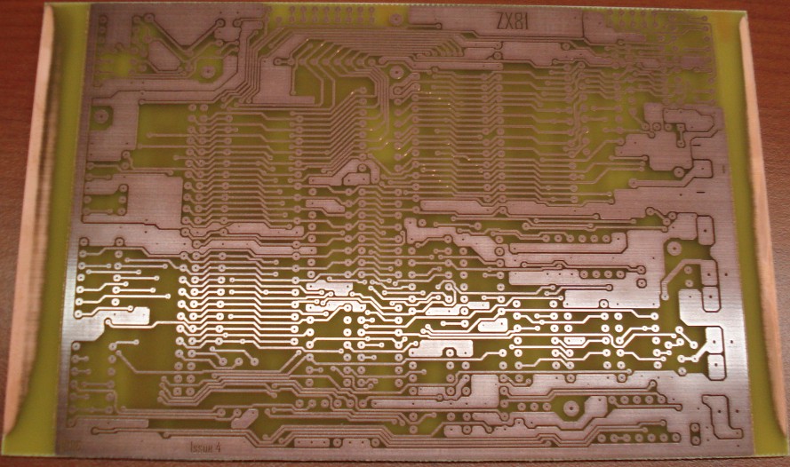
ZX81 Issue 4 bottom layer – just etched
As you can see, the photo sensitive layer is still on the PCB. Next is to cut off the sides, strip off the paint layer and start drilling the holes. After drilling the holes, you also could apply some flux spray which can protect your board and make soldering easier. I didn’t do that in these examples, but I think for my next PCB I will. The spray can protect the copper against the acid on your fingers a little bit which prevents corrosion of the copper surface. Another tip would be if available to use tin covered wire which is easier to solder as well.
ZX81 Issue 4 – Bottom Layer – cut, drilled, via wires just soldered
Here is a photo where you can see the small wires which I have ‘sewed’ in. This method of threading through the thin wire used for via connections back and forth saves us some time in inserting the via wires, as well as provides stably fastened wires which makes soldering easier. An advice here: try to anticipate the soldering job which is coming up next, and thread the wire through in such a way that the soldering job will not be so awkward and it will not be so easy to accidentally solder the wire to the wrong via or onto an adjacent trace.
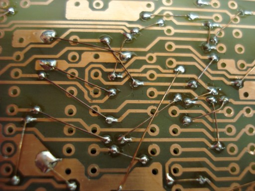
a close-up of the thin via wires which are threaded in
From this close up you can see what I mean. I tried as much as possible to thread the wire in such a way that the soldering job would not be hindered too much. After this phase is completed, the next job is cutting away the via wires now still present. For this job you should use a pair of cutters which have very small and somewhat pointy jaws which have the cutting area close to the edge of the jaws so you can easily get as near as possible to the vias and cut away the wires which as shortly as possible. The cross section of the cutters should be like this:
Finally the components need to be soldered in. This job should be done strategically by planning the progress of components step by step across the PCB, because we need to solder the components with the bottom as well as the top side of the PCB. Reaching the top wires/pins of the components is the important thing to keep in mind. During this top side soldering job it is best to keep a bright TL light source below the PCB and another one above it, preferable a light source with a magnifying glass integrated, or a light source above the PCB while keeping a magnifying glass on a stand next to the component which needs to be soldered. The more light you use on all sides, the easier the job will be. Also, TL light is much better than normal lamps.
First heat the pad and wire or component pin, then add the thin(0.35mm) solder wire to the pad and feed more solder while the solder flows to the pad and component pin until sufficiently covered. Make sure the soldering wire is always made straight again before soldering and the soldering iron’s tip is clean before each solder point. Otherwise when you touch a track next to the component it might catch the solder and become involved in the solder joint. When soldering the precision IC sockets, it’s absolutely necessary to seperate the two strips from eachother with a pair of cutters so you can reach the pins at the top much better. Another tip: insert another strip on top of the one you are soldering to hold down the pins. Otherwise they might rise up during soldering because the plastic might melt a bit. Later on there are a few more cautions: make sure to insert the ICs with correct orientation because they are not all facing up. Also, make sure when ever pulling an IC to really pull it with an IC extractor, and not using a screwdriver to wedge the IC out, otherwise you might damage the PCB or the IC socket. Some care should be used in that case because the IC sockets are not normal ones. After this phase of adding the components, it will be wise to have another short inspection, though I should say that the inspection should best take place directly after soldering each part or IC strip, because then you can give it more attention. The power connector if possible is best soldered to bottom and top layers to improve it’s connection to the PCB. For this purpose you can reach it from below and carefully solder the top tracks to it’s side. For the EAR, MIC and expansion connectors it’s not needed to solder the top pins. For the video output connector it is best to solder both top and bottom to ensure better mechanical strength. Remember, we will be plugging in the connector later on. Also at the bottom, the video connector’s pins should be bent to hold it even more strongly to the PCB.
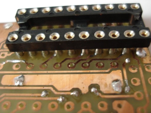
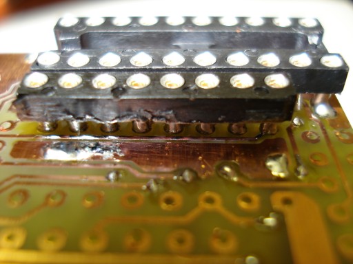
a close up of the first IC socket soldered in
From the photo you can see how I soldered the top pins of the socket onto the PCB pads. I used a needle tip soldering iron and thin 0.35mm solder wire, with bright TL light above and below the PCB to ensure no hidden short circuits. Remember to add the solder to the pad and pin and not onto the soldering iron’s tip itself, or the solder might catch onto an adjacent track.
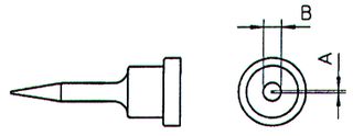
example diagram of needle tip for soldering iron
the second IC socket which is seperated into strips before soldering
Here you can see the first seperated strip soldered in, as you can see I started at the edge of the PCB, planning and working my way across the board, always anticipating to be able to reach the next parts to come. The strip here was a bit melted by the soldering iron’s heat, which can be expected with such a delicate job, while still getting used to the type of soldering work needed there. Later on I got more used to this work and it looked much better as I went along. Any imperfections can be cleaned up a little using a sharp hobby knife and very carefully cutting off melted the plastic edge sticking out. Then the result looks more neat. Make sure not to touch the tracks of the PCB with the knife.
The resistor network RN3 of the keyboard connector as used on this particular board only needs 5 resistors. In case you can only get a 8 resistor type, the remaining 3 resistors can be cut off. Make sure to cut through the resistor network a little further away from the last resistor you plan to keep, or the pressure of the cutters can cause the nearest resistor to increase it’s value. Just a little increase will not be a big problem though, it will still be usable. For this purpose I would advise using a bigger pair of cutters because these resistor networks are made from very strong material which could damage a small pair of cutters.
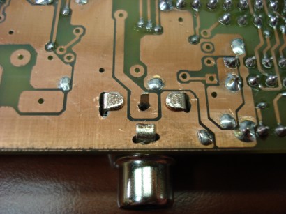
a close-up of the video connector just inserted into the PCB
The video output connector can be securely fastened by bending the connector’s legs to a right angle as shown in the photo. It’s best to cut off a little of the bottom leg as seen in the picture, so it won’t reach the centre pad.
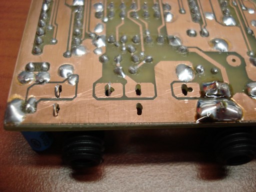
the original ZX81 connectors can be re-used on the ZX81 Issue 4 PCB
As shown in the photo above, the original ZX81 connectors for power, mic and ear can be soldered out from a ZX81 PCB and used for the ZX81 Issue 4. For making the holes as seen in the photo, I used a broken off hardmetal drill which still had a little bit of drilling area left on it. The drill is so strong (because it is very short now) that it can be used to cut larger areas out of a PCB. It is the type which has about 2,5-3mm diameter for most it’s length and only the end is 0.8mm. This 0.8 mm end on my drill is only about 1.5mm long so it’s not easy to break off and can be used in a sawing fashion.
Finally remains adding the ICs into the finished PCB. Remember the correct orientation according to the component placement diagram.

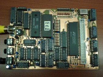
a larger picture of the finished prototype PCB
Here you can see the completed PCB. Observe the jumper positions and potmeter adjustment for a good initial test. As you can see from the photo, I have soldered out the original power, ear and mic connectors from an original ZX81 PCB. During desoldering, make sure to not heat the connectors too long because the plastic can easily melt. Note the resistors inserted into IC sockets which form the resistor networks for data and address bus seperation in certain areas of the schematic. Also have a look at the video connector here where you can see how I also soldered the connector to the top of the PCB for extra strength. It’s better to use this method because the connector entry is at a slightly higher point away from the PCB which can add more force to the fastening, also Cinch connectors tend to go into the bus a little harder than for example the 3,5mm connectors, so there is extra stress on the ‘bus’ part itself.
Testing went reasonably well. There was some problem with character display so I followed all the connections in this area of the schematic with a multimeter on the PCB, marking the checked connections with a coloured pen. Finally I found that one of the via’s didn’t make a good connection. I must have touched it during the soldering work of other components and it came out a little bit. After soldering a new wire in it was ok. Also I found a small problem with the keyboard connection to A8′ with a diode, apparently using this line with certain keys can cause a crash. After some testing I found that it is much more stable using a diode to the A8 line instead of A8′. I have corrected the schematic and PCB accordingly.
About video display: somehow the setting for white background with black text and white border can give a problem on the video monitor. The picture becomes very dark, even at the brightest potmeter setting. I tried it on two different TVs, one is a normal TV, another is a LCD TV, both have this problem. Strangely I distinctly remember that it worked fine one time before but not anymore now. It seems to be something related to the brightness level adjustment or calibration which occurs inside the tv circuits. Perhaps this adjustment or calibration is done in the blanking areas of television signals. I found it does work well when I remove the PAL jumper and the ZX81 operates in NTSC mode. Somehow the white level is correctly assumed by the TV in that case. Another solution is making the border black which is what I did in this case. (see photo above for jumper settings) Maybe later I can find the cause when I take the board to work where I can analyse the video signal with a scope. If I find some solution I will document it here. For now I am more than satisfied with the prototype because the video problem occurs in all my other ZX81 and ZX97 designs as well so it is a problem inherent to ZX81 video display in combination with TV video circuitry/technology. I seem to remember that when using a TV modulator this problem might be solved as well. Later on I might build a seperate TV modulator box which can be connected between the ZX81 and a television. Because of very limited space inside the ZX81 I could not include an optional modulator in this design.
In this prototype I used a 2764 EPROM because my supplier sent me some PLCC 27C256 EPROMS with my order, and I can’t seem to find my UV lamp for erasing some previously used EPROMS. Even though with a 2764 in the socket the /P line is pulled low and VPP is connected to 5V in this circuit, apparently the 2764 EPROM can operate fine, though of course not according to normal operating specifications. Sometimes we have to improvise something not-standard to get some results. 🙂 For now it keeps working fine. EPROMS are really solid components in my opinion. I tried to erase some EPROMS using my UV exposing unit for PCBs but even after an hour of exposing, no luck! 🙂 It must be the wrong wavelength or intensity.
Finally remains to wish you lots of fun and success in building this project.
ZX81 Issue 4 Schematic

ZX81 Issue 4 Component Placement
The copyrights of Sinclair Technology are the property of international computer manufacturer Amstrad. It is not allowed to use any designs provided in this website and/or any Sinclair Technology found elsewhere on the internet for any commercial use. It is not allowed to sell computers built with or based on plans from this website with the intent to make any commercial profit or gain. The sole purpose of the designs in this website is to use the designs for your hobby or for non-commercial learning purposes.