
The Euro-ZX81 is my first design which I made several years ago. At the time my most important concern was to create a working ZX81 as at the time I didn’t have many proven ZX prototypes yet. In fact, first I made the original ZX97, then next came a simple ZX80 -> ZX81 design which I finally split up more evenly into the Euro-ZX81 which consists of two 10×16 ‘euro-size’ PCBs. They are piggy backed on top of eachother into a nice space-saving design.
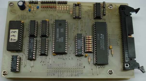
A picture of the Euro-ZX81 which consists of two PCBs piggy-backed onto eachother
Display Screen Type
The Euro ZX81 produces a black and white screen on a television set. I have included two jumpers in the design with which it’s possible to select the border and background color. (also see jumper descriptions) The Euro ZX81 has a Composite Video output which means you will need a seperate A/V input (Cinch, SCART, DIN, BNC etc.) on your TV to connect the video output of the Euro-ZX81.
Normally the Euro-ZX81 operates in character mode which means that only characters in the CHR$ set are displayed on the screen, however, since the ZX81 has been introduced, several High-res software solutions were invented that allow a high resolution display on the ZX81 of which every pixel is seperately programmable.
Tape Storage of your Programs
If you plan to use an audio device such as a cassette recorder or your PC soundcard for saving and loading, you can make use of the Euro-ZX81’s Tape input and output ports. The ‘EAR’ port(J3 on the CPU Board) is the ZX81’s audio input port, connected to the Earphone output of the cassette tape recorder, and the ‘MIC’ port(J4 on the CPU Board) is the ZX81’s audio output port, connected to the Microphone input of the cassette tape recorder(or PC).
I did use a different value in the circuit diagrams for some parts because with the R/C values as in the original Sinclair schematics I had problems recording programs through the MIC output. After some experimenting I got good results with the values as in the current circuit diagram.
Also there may be problems with the keyboard being slightly unreliable especially with long keyboard wires (capacitive), and also with loading programs from tape or PC soundcard. These problems could be solved by using a 74LS365A instead of a HC type for U10, which is the input port for both keyboard and tape input. An LS type will be much less sensitive.
Keyboard
For those not familiar with the ZX81 hardware, the keyboard that is used with the ZX81 is called a matrix keyboard. This means that all the keys used are mapped in a matrix position. When a ‘row’ line is connected to a ‘column’ line by a keyboard switch, it will be registered by the computer and the action that goes with this keypress will be executed by the computer. The ‘row’ signals are located in J7(CPU Board) and the ‘column’ signals in J6(CPU Board).
The row signals of J7 are then devided in two groups of 4 signals that pair up with the 5 column signals of J6 to make a block of 4×5 keys. Two of these blocks then add up to 40 keys total. The matrix keyboard is more clearly illustrated by the following table:
Block1  J6-1: J6-2: J6-3: J6-4: J6-5: Block2  J6-5: J6-4: J6-3: J6-2: J6-1:
J7-4:     1     2     3     4     5     J7-5:   6     7     8     9     0
J7-3:     Q     W     E     R     T     J7-6:   Y     U     I     O     P
J7-2:     A     S     D     F     G     J7-7:   H     J     K     L   Newline
J7-1:   Shift   Z     X     C     V     J7-8:   B     N     M     .   Space
Please note: most keys have several functions. These functions can be selected by the following methods:
1. Shift + Key
2. Shift + Enter: changes the cursor into a ‘F’ which is the ‘function mode’. In this mode, most keys have extra functions that are accessed by simply pressing the key after you have changed the cursor to ‘F’. After pressing a key, the ‘F’ cursor becomes a ‘K’ or ‘L’ cursor again.
3. Shift + 9: changes the cursor into a ‘G’ which is the ‘Graphics mode’. Keys pressed with a ‘G’ Cursor will result either in inverted text or in combination with shift some of them produce graphic symbols. The ‘G’ cursor will not change back by itself, you will have to press Shift + 9 again in order to change back to normal typing mode.
4. ‘K’ cursor mode. This mode results in a Keyword when certain keys are pressed.
5. ‘L’ cursor mode. This mode results in Letters when you press the letter keys. You can however still use Shift+Key and ‘F’ + Key in this mode which in some cases also produces keywords and functions.
Also note: the ZX81 handles the ‘K’ – ‘L’ cursor transitions automatically. For example, when you enter a keyword with the ‘K’ cursor, it changes to ‘L’ and you’re able to enter variables, mathematical symbols etc.
Jumpers/Options
JMP2 selects border color, and JMP1 selects character color, however note that JMP1 inverts the setting of JMP2 if changed.
For example, set both jumpers to 1-2 to make sure you can see the picture on the tv screen because with certain settings can be difficult to see the tv picture.
Diode D11 (CPU Board) selects the TV standard: do not place it when you want 50Hz (PAL, for example in Europe); Install it to get 60Hz. (NTSC, for example in the US)
Memory decoder
The ZX81 memory decoder operates as follows for the main memory blocks:
Memory-map
Mem Area: 0000-1FFF 2000-3FFF 4000-5FFF 6000-7FFF 8000-9FFF A000-BFFF C000-DFFF E000-FFFF
Normal:      ROM       RAM       RAM       RAM       RAM       RAM       RAM       RAM
/M1 low:     ROM       RAM       RAM       RAM       RAM       RAM       RAM*      RAM*
* during /M1 low, and certain other signal conditions, DFILE is read from RAM, and any memory access to the C000h-FFFFh area is redirected by the memory decoder to the 4000h-7FFFh RAM memory area. This is necessary to achieve proper display generation and continued stability while the ZX81 is executing programs in the higher RAM areas.
PCB Layout files
The PCB layouts are large PCX 1bit bitmap files. In order to save webspace, I have decided not to put these large files on the website, but instead you can email me and request the files. (be sure to mention which computer and which version you’re interested in) I will then respond as soon as possible with the requested file in an attachment.
As I mentioned on the ZX81 main page, the Euro-ZX81 consists of two euro sized (10x16cm) PCBs. The first board is the Euro-ZX81 CPU Board.
ZX81 Euro CPU Board
This chapter documents the information necessary to build the ZX81 CPU Board V2 which can pair up with the ZX81 Video Board V4 to make a functional Euro-ZX81 assembly. Click the links above or below to proceed to the schematic, component placement diagram and partslist pages.
Some Notes
This is the CPU Board V2, which means that it’s the third version. (starting from V0) It turned out that I didn’t need to update this board with the next revisions of the Video Board (V3 and V4), because there were no changes on this CPU board that warranted a PCB revision. During my updates of the entire Euro-ZX81 design I merely left out a few parts on this CPU Board to allow for more HC/HCT logic to work properly. It has been my strategy with the Euro-ZX81 to have as many HC/HCT ICs as possible, even though some ICs in the Euro-ZX81 need to be LS types. So we get a mix of LS/HC/HCT. I know some people consider this to be a bad idea and bad design, but remember that the original schematics were from Sinclair Research and a few other people who made the updates to upgrade to ZX81 functionality years ago. Basically these original designs, which I used as a basis for the Euro-ZX81, are the reason why there are some LS type ICs necessary in the Euro-ZX81. I don’t really mind this combination, I just keep in mind to have as much HC/HCT as possible, and where it isn’t possible I’ll use LS. The IC types are clearly marked on the partslist page and they should be exactly those types since I can’t guarantee that it will work if you use different ICs. Feel free to try any combinations, however, be warned that it could be difficult and there could be other unwanted side effects that are at first perhaps not even so clearly visible.
The parts that can be left out on the CPU Board are C33 and R2. These are not present in the partslist to avoid confusion. D11 should be used only if you want to use a NTSC television.(in the USA and Japan for example) If you leave it out, you will get a PAL video signal.
I used pieces of precision IC sockets as connectors on the board(see photo on main project page). They have many advantages, of which I find their relative small size and 0.8mm hole suitability most important. If I would use connectors that needed 1.0 or 1.25mm holes, the pads would have been much larger, so I would have had less space on the board. My single sided design technique is difficult enough as it is, so I always try to save space when I can. Also, these connectors have proven to be very reliable during my past years of prototype building.
ROM Image
The ROM image that I used to burn into the 27C64 EPROM is of course the standard ZX81 ROM. You can download the ROM image from this link.
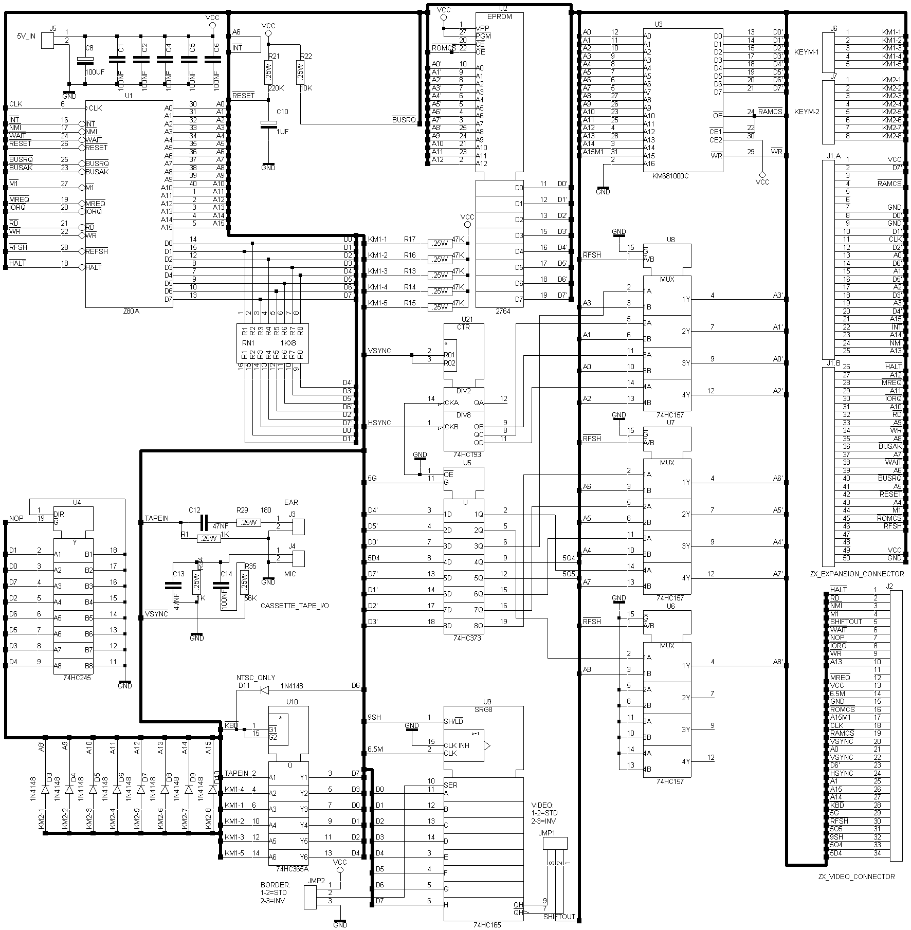
ZX81 Euro CPU Board Schematics:
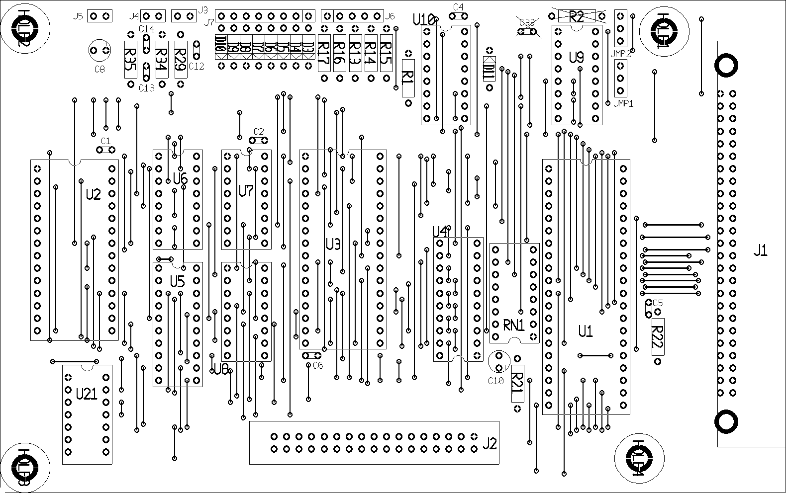
Euro ZX81 CPU Board Component Placement:
Euro ZX81 CPU Board Partslist:
U1 – Z80A CPU
U2 – 27C64 or 2764
U3 – KM681000C
U4 – 74HC245
U5 – 74HC373
U6 – 74HC157
U7 – 74HC157
U8 – 74HC157
U9 – 74HC165
U10 – 74LS365A
U21 – 74HCT93
D3-D10 – 1N4148
D11 – 1N4148 (NTSC optional)
C1, C2, C4, C5, C6 – 100nF
C8 – 100uF
C10 – 1uF tantal
C12, C13 – 47nF
C14 – 100nF
J1 – 50 pin FC connector
J2 – 34 pin connector
J3, J4, J5 – 2-Pin connector
J6 – 5-Pin connector
J7 – 8-Pin connector
JMP1 – 3-Pin connector
JMP2 – 3-Pin connector
R1, R34 – 1k
R13-R17 – 47k
R21 – 220k
R22 – 10k
R29 – 180
R35 – 56k
RN1 – DIP resistor network 8x1k
* J2 is the ZX81 Video Connector, a connector made from two 17 pin strips of precision IC Socket soldered onto the bottom(solder side) of the CPU Board. Make sure this connector has sufficient space from the pads on the solder side so you can solder it to the bottom of the PCB with a thin soldering tip. It is a good idea to always have a few pieces of IC socket strips inserted into those pins you’re about to solder so the heat will dissipate without melting the pins loose. Also, the pin strips you insert into the two connectors while soldering can hold them in place.
See the photo page (links on Euro-ZX81 page or CPU Board Page) for a photo of the bottom of the ZX81 CPU Board to illustrate the position of the connector strips and to have an idea what it looks like when soldered in place. The ZX81 Video Board has a similar set of female connectors, but they are soldered on the component side. Both boards are plugged together by a set of male-male precision connector strips, which provide enough space between the boards while assuring a perfect and reliable connection.
Euro ZX81 Video Board
About this Chapter
This chapter documents the information necessary to build the ZX81 Video Board V4 which can pair up with the ZX81 CPU Board V2 to make a working Euro-ZX81 assembly. Click the links above or below to proceed to the schematic, component placement diagram and partslist pages.
Some Notes
This is the Video Board V4, so it’s the fifth version. (starting from V0) It was necessary to revise this board several times before I could get the final bugs in the display out. As stated on the main ZX81 page, there is still a little problem with FAST mode where the character lines are somewhat rotated in order(delay problem), so the display appears a little funny in this mode, though it is still readable.
If you have a system configuration that operates constantly in FAST mode, for example a system which contains the ZX-Team LCD Interface where the ZX81 itself can operate in FAST mode while on the LCD the display is still in SLOW mode, then you can remove C23 so the display will be back to normal in FAST mode. Of course, when you go to SLOW mode without C23, the display will be slightly off similar to FAST mode with C23. SO only remove C23 if you’re sure you will only be working in FAST mode.
As I stated on the CPU Board page, my strategy has been to have as much HC/HCT ICs as possible but unfortunately not all original LS ICs could be replaced by HC/HCT, so make sure you follow the partslist accurately since I can’t guarantee good results in IC type combinations that differ from my partslist. Of course, you can always try your own combinations if you have other ICs than in my partslist, but be warned that you can run into problems. So the safest way to get the Euro-ZX81 up and running is to follow my partslists that are taken directly from my working prototype here. For more details why some ICs need to be LS types, read the Euro-ZX81 and Euro-ZX81 CPU Board pages.
You can see in the pictures(link below or on Pictures page) that I used pieces of precision IC socket as connectors on the board. They have many advantages, of which I find their relative small size and 0.8mm hole suitability most important. If I would use connectors that needed 1.0 or 1.25mm holes, the pads would have been much larger, so I would have had less space on the board. My single sided design technique is difficult enough as it is, so I always try to save space when I can. Also, these connectors have proven to be very reliable during my past years of prototype building.
Testing Info
There is a variable resistor on the Video Board, P1, which controls the video output intensity level. You can drill a hole underneath P1 so you will be able to adjust it while the boards are connected into an assembly. So if you can’t make out a picture on your tv, try adjusting P1 and turn up the intensity and contrast on your tv, until you can make out a picture on the tv. Then you can put the tv back to normal settings and try to get the picture to appear properly by adjusting P1 again. Also note that it’s a good idea to put both screen jumpers JMP1 and JMP2 on the CPU Board in position 1-2 to make sure you will have a white screen with black border which ensures that the ‘back porch’ of the video signal is a proper black level signal which in turn ensures proper contrast on the tv when you use its composite input. Later you can experiment all you want with several possible settings to see what you like and what works properly with your tv. If you use white screen and border, you may be able to improve the ‘back porch’ signal problem(which causes a very dark picture with the composite input) by using a tv modulator and the antenna input of the tv.
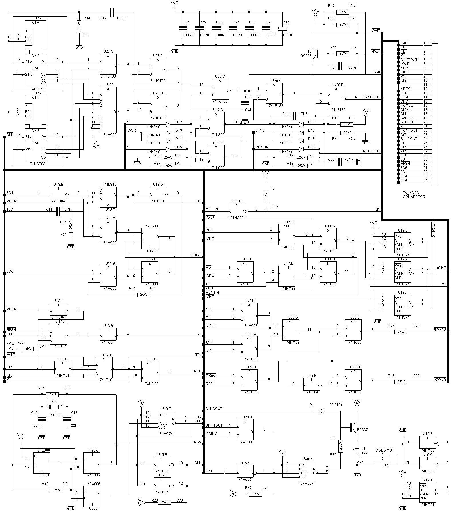
Euro ZX81 Video Board Schematics:
Euro ZX81 Video Board Component Placement: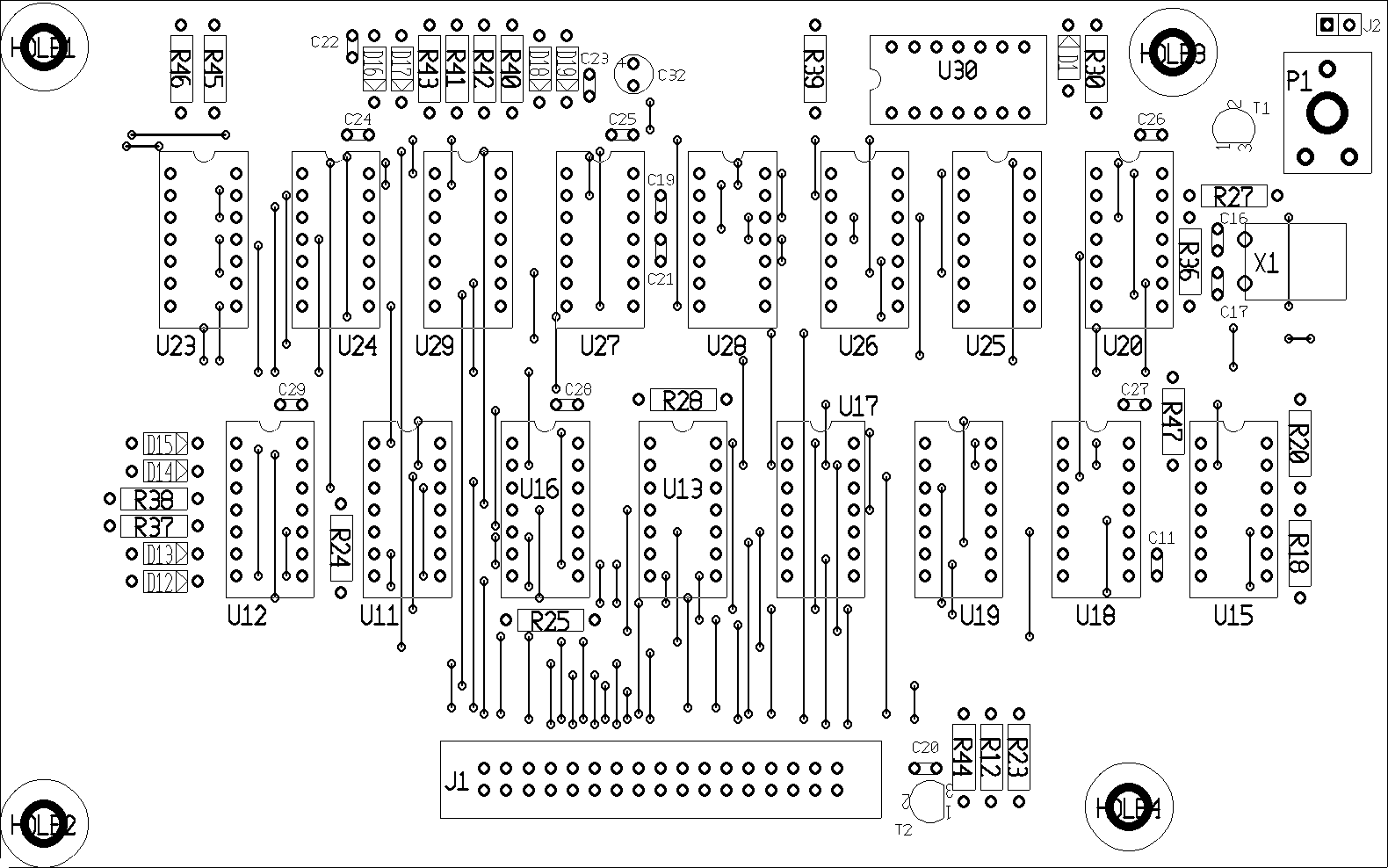
Euro ZX81 Video Board Partslist
U11 – 74HCT00
U12 – 74LS00
U13 – 74HC04
U15 – 74HC05
U16 – 74LS10
U17 – 74HC32
U18 – 74HC74
U19 – 74HC74
U20 – 74LS86
U23 – 74HC32
U24 – 74HC08
U25 – 74HCT93
U26 – 74HCT93
U27 – 74HCT00
U28 – 74HC30
U29 – 74LS132
U30 – 74HC74
D1 – 1N4148
D12-D19 – 1N4148
C11, C20 – 47pF
C16, C17 – 22pF
C19 – 100pF
C21 – 6.8nF *
C22, C23 – 47nF
C24-C29 – 100nF
C32 – 100uF
P1 – 220 ohms linear potmeter
T1, T2 – BC337
J1 – 34-pin connector
J2 – 2-pin connector
R12, R23, R44 – 10k
R18, R24, R27, R37, R38, R42, R43, R47 – 1k
R20, R30, R39 – 330 ohms
R25 – 470 ohms
R28, R41 – 47k
R36 – 10M
R40 – 4k7
R45, R46 – 820 ohms
X1 – 6.5 Mhz crystal
The copyrights of Sinclair Technology are the property of international computer manufacturer Amstrad. It is not allowed to use any designs provided in this website and/or any Sinclair Technology found elsewhere on the internet for any commercial use. It is not allowed to sell computers built with or based on plans from this website with the intent to make any commercial profit or gain. The sole purpose of the designs in this website is to use the designs for your hobby or for non-commercial learning purposes.